Recommended resources
The freely available resources this lesson will direct you to.
Introduction
In our previous lesson, we established a systematic method for finding the DC operating point (Q-point) in MOSFET circuits with passive resistors and ideal current sources. We saw that proper biasing is essential to prepare a transistor for amplification. Today, we will explore a technique that is fundamental to modern integrated circuit (IC) design: replacing bulky resistors with other transistors. Your learning goal is to analyze the DC operating point of a MOSFET circuit that uses another transistor as its load—a configuration known as an active load.
This is a crucial step in your study of analog circuits. In the world of microelectronics, where millions of transistors fit on a tiny silicon chip, a single resistor can be a space-hogging component. Using transistors as active loads not only saves precious chip area but, as we will see in later modules, also enables the design of amplifiers with exceptionally high voltage gain. This lesson will equip you with the analytical skills to determine the Q-point for these sophisticated and practical circuits.
Why Use Active Loads?
Before diving into the analysis, it's important to understand the motivation behind using a transistor as a load. In discrete circuits built on a breadboard, using a resistor is simple and effective. However, in an IC, the story is very different.
Mosfet Dc Biasing Techniques | Bohrium
This article from Bohrium provides an excellent conceptual overview of why active loads are so important in IC design.
Please read the paragraph that begins with this idea. It explains the core concept of replacing a large, space-consuming resistor with a compact transistor to create an amplifier stage with superior performance.
The key takeaway is that active loads are a cornerstone of modern analog IC design. They are more area-efficient and can provide much higher incremental resistance than a passive resistor, which is the key to achieving high voltage gain. Let's look at a practical justification.
[PDF] Integrated Circuit Design with the MOSFET
This textbook excerpt provides a compelling numerical argument for using active loads.
In the section titled "ACTIVE LOAD STAGE", find the text box labeled "PRACTICAL Considerations". Read this short paragraph to see how a moderately large resistor can create a DC voltage drop that is incompatible with typical low-voltage power supplies used in ICs.
This practical constraint makes passive resistors unsuitable for high-gain stages in ICs. The solution is to use a transistor, biased to behave like a current source, as the load.
Analyzing a Common-Source Amplifier with an Active Load
The most common active load configuration is a PMOS current mirror acting as a load for an NMOS common-source amplifier. Let's break down how to analyze its DC operating point.

The circuit shown above is a differential pair, but we can analyze one half of it (e.g., transistors Q1 and Q3) to understand the principles of a single common-source stage with an active load. Q3 is part of a current mirror, and it is biased to provide a specific DC current to the drain of the amplifying transistor, Q1.
The DC analysis hinges on one key principle: the drain current of the amplifying transistor must equal the current supplied by the load transistor.
Our goal is to find the DC output voltage, , and confirm the required input DC voltage, , that establishes the desired drain current, , while ensuring both transistors remain in the saturation region.
The following video provides a concise explanation of these operating conditions.
MOSFET: Common Source Amplifier with current source as load
This video from techgurukula, "MOSFET: Common Source Amplifier with current source as load," clearly explains how a PMOS transistor is used as an active load and what conditions must be met.
Please watch the segment from this point. The instructor first introduces the PMOS transistor as a practical current source and then derives the output voltage range required to keep both the NMOS and PMOS transistors in saturation.
As the video explains, for the circuit to function correctly as an amplifier, both transistors must be in saturation. This imposes two critical conditions on the DC output voltage, :
-
For the NMOS amplifier (M1) to be in saturation: The drain-source voltage must be greater than its overdrive voltage.
Since , this sets the lower limit for the output voltage: -
For the PMOS load (M2) to be in saturation: Its drain-source voltage, , must be greater than its overdrive voltage.
Since , this can be rearranged to find the upper limit for the output voltage:
So, .
The DC operating point must lie within this valid range: .
A Step-by-Step Analysis Example
Let's apply these concepts to a concrete problem. The procedure is an extension of the five-step method from our last lesson. We'll assume both transistors are in saturation, equate their drain currents, and solve for the unknown voltages.
We'll use a slightly different circuit configuration to broaden your experience, but the core principles are identical. In this problem, an NMOS current mirror sources current into a pair of series-connected NMOS transistors.
MOSFET Solved Problem | Quiz # 338
This "MOSFET Solved Problem" from the ALL ABOUT ELECTRONICS - Quiz channel provides an excellent, clear walkthrough that reinforces the DC analysis technique.
Follow the instructor's logical steps to solve for the output voltage: Analyze the Current Source: First, watch how he identifies the current mirror and determines the current it supplies to the rest of the circuit at the start. This is I_{DQ}. Determine Node Voltages: Next, follow the KVL calculations to find the gate voltages for transistors M3 and M4 in this segment. Equate Currents and Solve: Finally, and most importantly, observe how he applies the core principle: since M3 and M4 are in series, their drain currents must be equal (I_{D3} = I_{D4} = I_{DQ}). By equating their saturation current equations, he solves for the output voltage.
The key insight from this problem is that once you know the DC bias current, the rest of the analysis involves applying the saturation I-V equation and basic circuit laws (KVL, KCL). The fact that the load is an active transistor simply means its current is determined by its own and device parameters, rather than by Ohm's law through a resistor.
Let's consider one more detailed example, which is very typical of a university exam question.
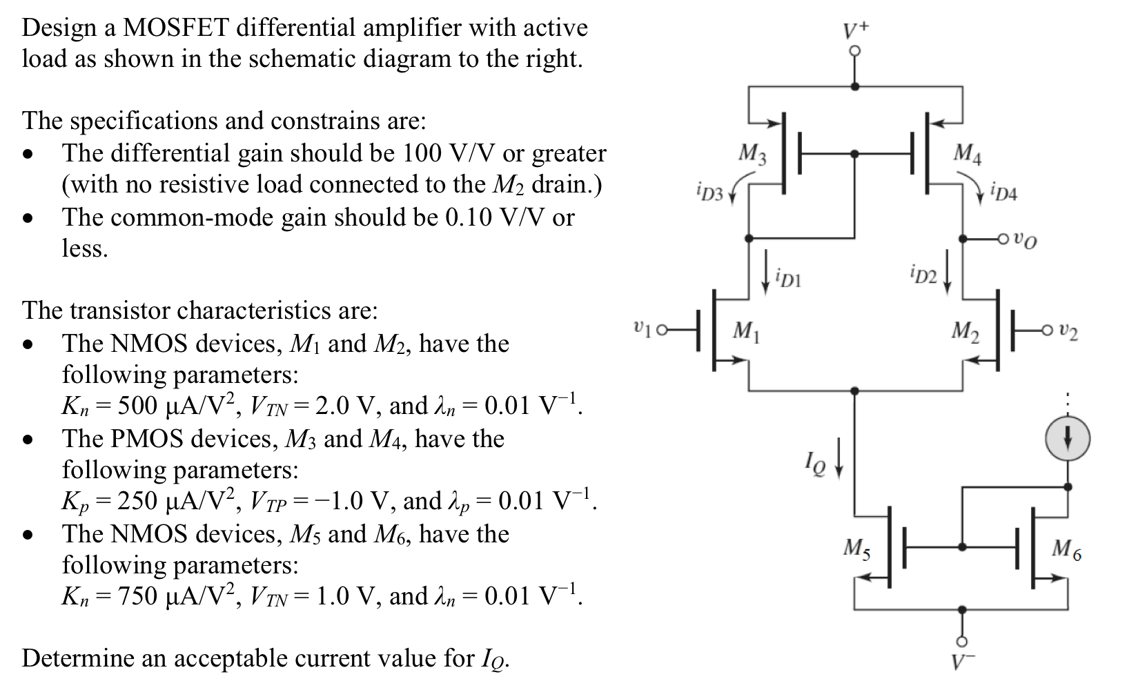
The problem asks to design the circuit, but we can use it for an analysis exercise. Let's assume we are given that the bias current . In a differential pair, this current splits equally, so the quiescent drain current for each branch is .
The circuit has PMOS transistors M3 and M4 forming a current mirror load for NMOS transistors M1 and M2. To find the Q-point of the right-hand side (M2 and M4), we proceed as follows:
- Assume Saturation: Assume M2 and M4 are in saturation.
- Enforce Currents: We know .
- Analyze PMOS Load: For the PMOS transistor M4, we have:
With , , and , we can solve for .
- Analyze NMOS Amplifier: For the NMOS transistor M2, we have:
With , , and , we can solve for .
This is the required DC gate-source voltage at the input to set the desired 100 A current. The Q-point current is . The Q-point output voltage, , would depend on the supply voltages and , which are not given here, but this process demonstrates how the transistor currents and voltages are linked.
Conclusion
In this lesson, you have moved from analyzing circuits with simple passive loads to understanding the DC behavior of amplifiers with active loads. This is a significant step towards mastering the design of modern integrated circuits.
Here are the main takeaways:
- Active loads (transistors used as loads) are preferred in ICs to save space and enable high-gain amplifier designs.
- A common implementation is a PMOS current mirror loading an NMOS amplifying transistor.
- DC analysis is centered on the principle of equating the drain currents of the amplifier and load transistors ().
- To find the Q-point and valid operating range, you must apply the saturation conditions for both the amplifying and the load transistors, which defines the allowable swing for the DC output voltage.
In our next lesson, we will pivot from analysis to design. Armed with the ability to determine the Q-point of a given circuit, you will learn how to choose the component values and transistor sizes needed to achieve a specific, desired DC operating point, a core skill for any circuit designer.