Hello! Welcome back to our series on embedded communication protocols.
In the last two lessons, we configured the SPI peripheral and implemented blocking functions to exchange data, establishing a solid foundation in synchronous communication. You learned how to manage multiple slaves with chip select and use HAL functions to transmit and receive data in a full-duplex manner.
Today, we shift our focus to the second major synchronous protocol you'll encounter constantly in the industry: I2C (Inter-Integrated Circuit). This lesson is dedicated to achieving a single, crucial learning outcome: Configure the I2C peripheral in master mode. We'll explore the protocol's theory and then walk through the configuration process on your STM32F103 board, preparing it for the data transactions we'll implement in our next session.
1. I2C Protocol Fundamentals
Before we touch any registers or configuration tools, it's essential to understand what makes I2C different from SPI. While both are master-slave synchronous protocols, their hardware implementation and protocol rules are distinct.
I2C uses only two wires:
- SDA (Serial Data): A bidirectional line for transferring data.
- SCL (Serial Clock): The clock line driven by the master.
The most significant hardware difference is that these lines are open-drain. This means that devices on the bus can only pull the line LOW. They cannot drive it HIGH. To bring the line HIGH, external pull-up resistors are required. This design is what allows multiple masters to coexist on the same bus without causing electrical conflicts.
To get a clear visual understanding of the I2C protocol, including the start/stop conditions and addressing scheme that we'll use in the next lesson, please watch the following segment.
Using I2C for any device on STM32 with HAL | VIDEO 26
This video from Matej Blagšič provides a concise and clear explanation of the fundamental I2C concepts.
Watch from 01:35 to 07:46. Focus on understanding the role of the SDA, SCL, and pull-up resistors. Pay close attention to the visual explanation of Start/Stop conditions, 7-bit addressing, and the Read/Write bit. This is the 'language' our configured peripheral will speak.
2. Configuring I2C in Master Mode: The STM32CubeIDE Approach
Just as with SPI, the fastest and most common way to configure peripherals is using the STM32CubeIDE graphical tool. This automates the register configuration and generates initialization code for you.
The process involves three main steps:
- Enable the Peripheral: In the "Connectivity" section, you select the I2C instance you want to use (e.g., I2C1).
- Configure I2C Settings: You set the communication speed. For most applications, you'll start with Standard Mode (100 kHz) or Fast Mode (400 kHz).
- Pin Assignment: The tool automatically assigns the correct GPIO pins (PB6 for SCL and PB7 for SDA on I2C1 for many STM32F1s) and configures them as Alternate Function Open-Drain.
The following image and video illustrate this process.
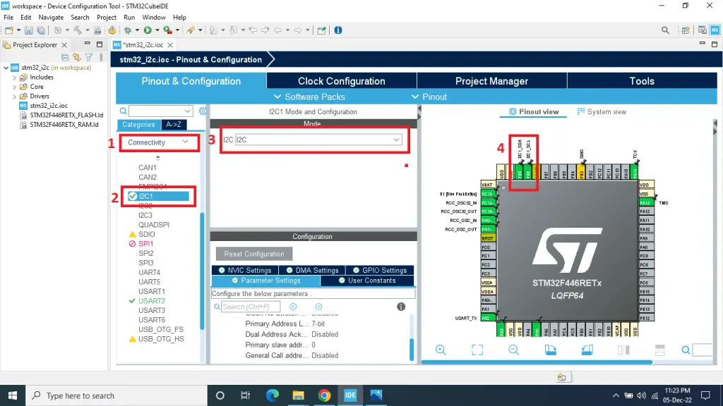
To see this in action, watch this short clip.
Using I2C for any device on STM32 with HAL | VIDEO 26
Let's watch Matej Blagšič demonstrate this configuration in STM32CubeIDE.
Watch from 14:24 to 15:50. Observe how the I2C1 peripheral is enabled and how the standard 100 kHz mode is selected. Notice that the pins PB6 and PB7 turn green, confirming their assignment.
When you generate the code, CubeIDE creates a function, typically MX_I2C1_Init(), which contains all the HAL function calls needed to set up the peripheral according to your graphical selections.
3. Under the Hood: Register-Level I2C Configuration
To meet professional standards, it's not enough to just click buttons in a GUI. You need to understand what that GUI is doing. Let's break down the exact register-level steps that the MX_I2C1_Init() function performs. This knowledge is invaluable for debugging and for working on projects that don't use CubeIDE.
The process follows a strict sequence defined in the STM32 reference manual.
I2C Communication in STM32 (PART1) | Register Programming Explained #4
The video 'I2C Communication in STM32 (PART1)' from ControllersTech is an excellent resource that walks through the register-level configuration step-by-step, referencing the manual as it goes.
Watch from 02:13 to 14:23. This is the core of our lesson. Follow along as the presenter covers each of the following configuration stages. You don't need to memorize the register bits, but you should understand the purpose of each step.
Let's summarize the key steps shown in the video:
Step 1: Enable Clocks (RCC Registers)
Before you can use any peripheral or GPIO, its clock must be running.
- Enable GPIO Clock: For I2C1 on the Blue Pill (PB6/PB7), you must enable the clock for
GPIOBin theRCC_APB2ENRregister. - Enable I2C Clock: The I2C1 peripheral is on the APB1 bus, so you must enable its clock in the
RCC_APB1ENRregister.
Step 2: Configure GPIO Pins
The pins must be correctly configured for I2C. For PB6 and PB7:
- Mode: Set to Alternate Function.
- Output Type: Set to Open-Drain. This is critical for I2C.
- Pull-up/Pull-down: Configure with an internal pull-up (though external pull-ups are often preferred for better signal integrity).
- Alternate Function Selection: Map the pins to the I2C1 function using the
AFRregisters.
Step 3: Configure I2C Timing Registers
This is where you define the communication speed.
I2C_CR2Register: You must tell the I2C peripheral the frequency of the APB1 clock it's running on. This is done by writing the frequency in MHz (e.g., '8' for the default 8MHz HSI) into theFREQbits ofCR2. The peripheral uses this value to calculate its internal timings.I2C_CCRRegister (Clock Control Register): This register determines the SCL clock frequency. Its value is calculated based on a formula in the reference manual involving the APB1 clock period and the desired I2C period. The video walks through this calculation for Standard Mode.

I2C_TRISERegister (Rise Time Register): This register is configured to account for the maximum rise time of the SDA and SCL signals, ensuring the protocol timing is respected.
Step 4: Enable the Peripheral
The final step is to bring the peripheral out of reset and enable it by setting the PE (Peripheral Enable) bit in the I2C_CR1 register.
The article "Getting Started with STM32F103: I2C Bus Scanner" on the Embedded Expert blog provides a concise bare-metal i2c_init() function that implements these register-level steps in C code. You can review sections 2.2 and 2.3 of that article to see the final code structure.
Conclusion
Congratulations! You have now learned how to configure the I2C peripheral for master mode operation from two essential perspectives: the high-level graphical tool and the low-level register manipulation that underpins it.
Key Takeaways:
- I2C is a two-wire (SDA/SCL), open-drain protocol that requires pull-up resistors.
- High-level configuration is done in STM32CubeIDE by enabling the peripheral, choosing a speed (e.g., 100 kHz), and letting the tool assign and configure the GPIOs as Alternate Function Open-Drain.
- Low-level configuration involves a precise sequence:
- Enable GPIO and I2C clocks in the RCC.
- Configure GPIO pins for Alternate Function Open-Drain.
- Set the APB1 clock frequency in
I2C_CR2. - Calculate and set timing values in
I2C_CCRandI2C_TRISE. - Enable the peripheral by setting the
PEbit inI2C_CR1.
- Understanding the register-level process is key to becoming a professional firmware developer, especially for debugging and optimization.
Preview of the Next Lesson:
With our I2C peripheral correctly configured and enabled, we are ready to communicate. In the next lesson, we will implement I2C master write and read transactions. You will learn to use HAL functions like HAL_I2C_Master_Transmit and HAL_I2C_Master_Receive to send data to and receive data from an I2C slave device, applying your knowledge of addressing and start/stop conditions to talk to the I2C LCD in your kit.