Recommended resources
The freely available resources this lesson will direct you to.
- How Silicon Wafers Are Made: 🔬From Sand to Smartphone Power📱#siliconwafers #semiconductor #waferwww.youtube.com
- 2.3: Crystallography (Single Crystal vs. Polycrystalline)www.youtube.com
- 4.2: Silicon Growth - Engineering LibreTextseng.libretexts.org
- 1.3: Crystals - Engineering LibreTextseng.libretexts.org
Welcome back. In the previous lesson, you traced the broad journey from a verified circuit design to a fabricated wafer, tested dies, and a packaged chip. We now zoom in on the material at the beginning of that journey: the wafer.
A wafer is not simply a thin slice of “silicon from sand.” It is an engineered starting platform whose chemical composition and atomic structure must be tightly controlled before billions of transistors and wires can be built on it. This lesson explains the two essential requirements: ultrapurity and single-crystal structure.
A semiconductor must be controllable, not merely conductive
Silicon is useful because its electrical behavior lies between that of a metal and an insulator. In a silicon crystal, each atom shares electrons with four neighboring atoms through covalent bonds. The regular arrangement produces an energy structure in which electrons normally remain bound, but can be made mobile under the right conditions.
That behavior is valuable only if it is predictable.
A transistor works by controlling the concentration and movement of charge carriers in very specific regions. Chipmakers deliberately introduce tiny, measured quantities of selected atoms, called dopants, to create regions with desired electrical properties:
- A donor dopant such as phosphorus can contribute an extra mobile electron, producing n-type silicon.
- An acceptor dopant such as boron can create an electron vacancy, or hole, producing p-type silicon.
These are intentional changes. Unwanted atoms are different: they may add carriers where none were intended, capture carriers, increase leakage current, interfere with thin-film growth, or cause different transistors on the same die to behave differently.
The crucial distinction is therefore:
| Material condition | What it means for fabrication |
|---|---|
| Intentional dopant | A known species, concentration, and location used to create a device function |
| Unwanted impurity | An uncontrolled species or concentration that changes behavior unpredictably |
| Ultrapure silicon | A highly controlled baseline from which precise electrical regions can be created |
A wafer does not need to be chemically “perfect” in an absolute sense. It needs impurities, dopants, crystalline defects, and contamination to be low enough and well characterized enough that process engineers can reliably predict the result of every later fabrication step.
Why ordinary silicon is far too impure
Silicon is abundant in nature, commonly found as silicon dioxide in sand and quartz. But abundance is not suitability. The first industrial reduction step produces metallurgical-grade silicon, which is useful for many applications but much too impure for integrated circuits.
The scale of the problem is striking. A cubic centimeter of crystalline silicon contains about atoms. Even a small impurity population relative to that enormous total can change the electrical properties of the material. The Engineering LibreTexts account frames the requirement as better than one part in , or 99.999999% purity, for electronic applications.
4.2: Silicon Growth - Engineering LibreTexts
Read “Silicon Growth” from Engineering LibreTexts to connect the apparently extreme purity requirement with the chemical purification and crystal-growth steps that produce wafer material.
In Section 4.2, begin at the paragraph that starts “We have seen that on the order of.” Read the purity argument through the explanation of why metallurgical-grade silicon is inadequate. Then continue through the discussion of trichlorosilane and fractional distillation, noting that purification works because different chemical compounds have different boiling points. Next, find the later paragraph beginning “Although the EGS is relatively pure.” Read the crystal-growth account. Focus on the important transition: electronic-grade silicon can be very pure yet still not be suitable as a device wafer until it is converted into one continuous crystal.
Purification does not simply mean repeatedly washing sand. Manufacturers convert silicon into chemical compounds such as trichlorosilane, separate unwanted compounds through processes such as fractional distillation, and then deposit highly purified electronic-grade silicon.
This chemical route matters because a contaminant such as iron, carbon, aluminum, or uncontrolled phosphorus cannot be tolerated merely because its quantity seems small by everyday standards. At transistor dimensions, microscopic contamination can become electrically significant.
Purity alone is not enough
Imagine two silicon pieces with the same chemical purity.
- The first consists of many small crystals joined together.
- The second is one uninterrupted crystal extending through the entire wafer.
The first is polycrystalline silicon. Each small crystal, or grain, has the same basic atomic arrangement but a different orientation. Where two grains meet, there is a grain boundary: an irregular interface where the atomic pattern cannot continue smoothly.
The second is single-crystal or monocrystalline silicon. Its atomic lattice retains one orientation across the usable wafer.
| Polycrystalline silicon | Single-crystal silicon |
|---|---|
| Contains many grains with differing orientations | Has one continuous lattice orientation |
| Contains grain boundaries between grains | Has no grain boundaries within the wafer crystal |
| Electrical behavior can vary around boundaries | Electrical properties are much more uniform across the wafer |
| Useful in some semiconductor structures | Essential starting material for mainstream high-performance silicon device fabrication |
Grain boundaries are problematic because they introduce locations where the regular bonding structure is disrupted. These sites can trap charge carriers, increase leakage, scatter carriers, and make transistor characteristics less uniform. A transistor that happens to cross or sit near such a boundary may not match one fabricated elsewhere on the wafer.
Uniformity is essential because fabrication is a repeated, high-precision process. A foundry does not want one transistor to work well only because it landed in a favorable grain and another to fail because it encountered a boundary. It needs the wafer to respond consistently to oxidation, doping, etching, heat treatment, and electrical fields.
A single crystal does not mean a wafer has literally no defects of any kind. Real wafers can contain defects and residual impurities, and controlling them is a major manufacturing challenge. Rather, “single crystal” means that the wafer is not an assembly of differently oriented crystal grains.
Growing one large silicon crystal
The most common method for producing mainstream silicon wafers is the Czochralski process, often abbreviated as the CZ process.
Highly purified electronic-grade silicon is melted in a crucible. A small, carefully oriented seed crystal is touched to the molten silicon and then slowly pulled upward while the system rotates under controlled thermal conditions. Silicon atoms at the solidification interface follow the seed’s atomic arrangement. Over time, the seed becomes a long cylindrical single crystal called an ingot or boule.
How Silicon Wafers Are Made: 🔬From Sand to Smartphone Power📱#siliconwafers #semiconductor #wafer
Watch “How Silicon Wafers Are Made: From Sand to Smartphone Power” by Mr. SMART Engineering for a compact visual account of the transition from raw silica to a single-crystal silicon ingot.
Begin with the wafer role to establish why a wafer must be highly pure and structurally sound. Then watch the purification route, concentrating on the difference between metallurgical-grade and electronic-grade silicon. Finish with crystal growth; pay particular attention to the seed crystal, controlled pulling, and the reason the resulting ingot has no grain boundaries.
The seed is more than a handle for pulling silicon from a melt. It establishes the orientation of the growing lattice. Control of temperature, pulling rate, rotation, and atmosphere determines whether the ingot grows with the desired diameter and crystal quality.
The wafer-production overview below puts this stage in the larger physical workflow. It begins with purified silicon feedstock, shows crystal pulling to create an ingot, then slicing and finishing to create the wafer on which circuits will eventually be fabricated.
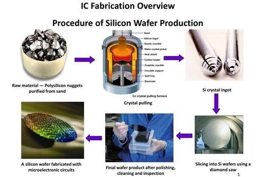
After growth, the ingot is processed into wafers. Broadly, manufacturers:
- Slice the ingot into thin disks using precision saws.
- Shape and smooth the wafer edges.
- Flatten and polish both surfaces to achieve an extremely smooth, uniform substrate.
- Clean and inspect the wafers before they enter fabrication.
The circular wafer is therefore the end product of a materials-engineering sequence, not the raw material itself.
Why single-crystal wafers support repeatable chipmaking
A fabricated chip contains millions to billions of devices, and the devices must operate within narrow electrical limits. Starting with ultrapure, single-crystal silicon gives process engineers a stable baseline in four connected ways.
1. Uniform electrical starting behavior
A regular crystal lattice supports more uniform carrier movement and more reproducible electrical behavior. This is the basis on which later doping steps create designed n-type and p-type regions.
2. Controlled doping
Fabrication deliberately changes only selected locations on the wafer. If the starting material already contains uncontrolled electrically active impurities, the final doping concentration becomes less predictable. The same implanted dose could produce different transistor behavior in different places.
3. Consistent processing
Later steps depend on the substrate’s surface and atomic arrangement. A uniform crystalline starting material helps engineers achieve repeatable results in processes such as thermal oxidation and high-temperature treatments. Process recipes can be developed around a known substrate rather than compensating for random grain-to-grain variation.
4. Better yield and reliability
A defect or variability source in the substrate can affect many devices built above it. In dense modern circuits, small deviations can become leakage paths, timing variation, or early reliability failures. Material quality therefore contributes directly to the fraction of dies that function correctly after fabrication.
This is why “silicon wafer” should not be treated as a generic blank canvas. It is a carefully produced, electronically controlled foundation. The later layers of insulators, conductors, and patterned transistor structures can only meet their tight specifications if this foundation is sufficiently pure, uniform, flat, and clean.
Key takeaways
Semiconductor fabrication begins with ultrapure, single-crystal silicon because the wafer must provide a known and uniform electrical starting point.
- Ultrapurity prevents uncontrolled atoms from changing carrier concentrations, increasing leakage, or disrupting later processing.
- Intentional doping is not a contradiction to purity: it is the precisely measured placement of selected atoms after establishing a controlled baseline.
- Single-crystal silicon has one continuous atomic lattice orientation, unlike polycrystalline silicon, which contains grains and grain boundaries.
- Grain boundaries can create electrical and process variability, making them unacceptable in the active substrate of mainstream integrated circuits.
- The Czochralski process grows a large single-crystal ingot from purified silicon and a seed crystal; the ingot is then sliced and polished into wafers.
Next, we will consider a related but separate problem: even an excellent wafer can be ruined by particles, chemicals, or human contamination. We will examine how cleanrooms, protective clothing, and wafer-cleaning steps protect the wafer throughout fabrication.