Recommended resources
The freely available resources this lesson will direct you to.
Welcome back. Last lesson established why a wafer begins as ultrapure, single-crystal silicon: the bulk material must provide a uniform, predictable foundation for every device built above it. This lesson shifts from the wafer’s interior to its exposed surface and surrounding environment.
During fabrication, a wafer repeatedly acquires films, patterns, and chemically modified regions. At each stage, a speck of dust, a trace metal ion, an organic film, or residue from the previous step can alter the intended result. We will examine the three coordinated defenses that keep this under control: the cleanroom, protective clothing and disciplined handling, and wafer-cleaning processes.
Contamination is not merely visible dirt
In ordinary life, a surface may look clean even when it is covered with molecules, trace residues, and particles far too small to see. For semiconductor manufacturing, “clean” means something much stricter: the wafer surface and its environment must meet limits for particles and chemical contaminants that could affect the next process.
The important distinction from the previous lesson is:
- Bulk impurities are unwanted atoms inside the silicon crystal before fabrication begins.
- Surface contamination is unwanted material deposited on the wafer during storage, handling, or processing.
- Process residue is material left over from a deliberately performed fabrication step.
All three can harm a chip, but they are controlled in different ways.
| Contaminant type | Typical sources | Why it can matter |
|---|---|---|
| Particles | Dust, clothing fibers, skin flakes, tool wear | Can block a pattern, prevent a film from adhering, or create a defect in a tiny structure |
| Organic contamination | Fingerprints, skin oils, packaging polymers, photoresist residue | Can interfere with surface reactions and coating uniformity |
| Metallic or ionic contamination | Tools, chemicals, containers, corrosion products | Can alter electrical behavior, cause leakage, or create charge traps |
| Airborne molecular contamination | Organic vapors and inorganic gases | Can adsorb on surfaces and disturb sensitive lithography or film-growth reactions |
A particle need not be large to be destructive. If it lands where a transistor’s insulating layer or electrical connection must be continuous, it can produce an open circuit, a short circuit, abnormal leakage, or an unreliable device. Metal atoms are especially problematic because heat treatments can drive them into silicon, where they may alter carrier behavior.
The effect is cumulative: a wafer is processed through many layers and many tools. A defect introduced early can remain embedded beneath later layers, making it impossible to repair.
A cleanroom controls the environment, rather than simply cleaning it
A cleanroom is a controlled manufacturing environment, not just an unusually tidy room. Its temperature, humidity, particle levels, airflow, and often pressure relationships with neighboring areas are managed so that contamination is less likely to reach critical wafer-processing locations.
The cleanroom “class” or rating specifies an allowable concentration of airborne particles at defined particle sizes. More sensitive steps require tighter limits, but the central idea is consistent: particle concentration is measured and limited, not assumed.
Watch “300mm wafer fab virtual tour” from Texas Instruments for a quick view of a working wafer-fab cleanroom. It connects the abstract idea of contamination control to the garments and air-handling infrastructure used around real wafers.
Watch the cleanroom introduction. Focus on the two complementary controls: garments that contain contamination from people and air purification that continually removes airborne particles.
A cleanroom uses several overlapping measures:
-
Filtered air. High-efficiency particulate air filters, often called HEPA filters, remove fine airborne particles. More demanding areas may use still more stringent filtration.
-
Controlled airflow. Air is delivered in a planned direction so that particles are carried away from sensitive work zones rather than wandering unpredictably in turbulent eddies.
-
Pressure zoning. Cleaner zones are commonly maintained at a pressure that discourages unfiltered air from leaking inward when doors or pass-throughs are used.
-
Low-shedding construction. Smooth, cleanable surfaces and carefully chosen materials reduce particle release and chemical outgassing from the facility itself.
-
Restricted, standardized behavior. Entry routes, gowning areas, equipment layouts, and movement rules reduce opportunities to carry contamination into the manufacturing area.
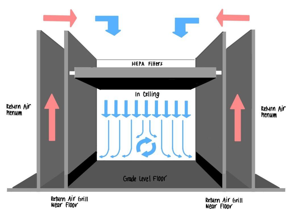
The cleanroom airflow diagram depicts a common vertical unidirectional-flow concept. Filtered air enters from the ceiling, flows generally downward past the wafer-processing region, and exits near the floor. This makes practical sense: particles released by a person or tool are more likely to be swept down toward returns than to remain suspended around the wafer.
The drawing is simplified. In an actual fab, equipment, workers, and wafer carriers can disturb airflow. Engineers therefore pay close attention to tool placement, airflow speed, filter maintenance, and the small controlled environments around especially sensitive processing equipment. Air filtration reduces the background risk; it does not make careless handling harmless.
Contamination Control in Semiconductor Fabrication Plants
Read this overview from Radley Engineering to consolidate the facility-level and human-level logic of contamination control. Treat it as a systems view: contamination must be prevented at its source, kept out of critical areas, and removed when it does appear.
In “How Are Cleanrooms Designed to Control Contamination?”, read the cleanroom-design overview, then continue through the subsections “What Cleanroom Classifications Are Used in Semiconductor Fabs?” and “How Do HVAC and Filtration Systems Reduce Contamination?” Focus on why filtration alone is insufficient without controlled airflow and materials. Next, in “How Do Operational Practices Reduce Human-Generated Contamination?”, read the personnel-control discussion. Pay attention to the connection among garments, controlled entry, training, and consistent movement.
Protective clothing contains the largest moving contamination source: people
Humans continuously shed skin cells, hair fragments, fibers, oils, and respiratory droplets. Everyday clothing sheds fibers as it moves, and ordinary shoes collect debris from the floor. A person can therefore carry and generate contamination even if they have just showered and their clothes look perfectly clean.
Cleanroom garments are designed mainly to protect the wafer from the person. They are also part of normal workplace safety practice, but their contamination-control purpose is containment.

The basic logic of gowning is to cover each major emission path:
- A hood or cap contains hair and particles released from the head.
- A face mask limits respiratory droplets and particles from speech, coughing, or breathing near a work area.
- A full cleanroom suit contains fibers and skin particles shed from clothing and the body.
- Gloves prevent transfer of skin oils, salts, and particles from hands.
- Boots or shoe covers prevent tracked-in floor contamination from becoming airborne or reaching equipment.
Gowning is only effective if it is performed correctly. For example, allowing a sleeve to touch the floor before touching a wafer carrier can transfer floor debris to the hand zone. This is why fabs use defined gowning sequences, designated benches, air showers in some facilities, and rules about cosmetics, personal items, and movement.
A useful way to interpret the protective suit is as a containment barrier, not a magical source of cleanliness. A damaged glove, an improperly closed hood, or a contaminated garment can itself become a source. For this reason, gowning, glove changes, and tool handling are standardized procedures rather than matters of personal preference.
Automation provides another layer of protection. Wafers often travel in closed carriers and are loaded into tools by robotic systems. Reducing direct handling reduces the opportunities for fingerprints, airborne shedding, accidental contact, and mishandling.
Wafer cleaning restores a controlled surface before critical steps
Even a highly controlled cleanroom cannot guarantee that every wafer remains chemically pristine. A wafer can accumulate residues from earlier processing, particles from tools, trace metal contamination from chemicals or containers, and a thin native oxide after exposure to air.
Wafer cleaning is therefore performed before selected critical steps and between process stages. It is not one universal wash. The appropriate clean depends on what is currently on the wafer and what process comes next.
For example, a wafer about to undergo high-temperature oxidation, deposition, or dopant diffusion needs an especially well-controlled surface. A contaminant that would be relatively harmless at room temperature may become incorporated into a film or driven into silicon during heating.
The traditional RCA clean is an influential family of wet-cleaning steps. Modern fabs use many refinements and proprietary variants, but its logic remains foundational:
| Cleaning purpose | General approach | Contamination addressed |
|---|---|---|
| Remove organic films | Oxidizing and alkaline cleaning chemistry | Oils, photoresist residues, many organic films |
| Remove particles | Chemical cleaning, rinsing, and sometimes megasonic agitation | Loosely bound particulate matter |
| Remove surface oxide when required | Brief oxide-removal treatment | Native oxide or oxide formed in an earlier cleaning stage |
| Remove metal ions | Acidic oxidizing chemistry that keeps dissolved metals from redepositing | Trace metals and alkali ions |
| Prevent residues after cleaning | Ultrapure-water rinse and controlled drying | Remaining chemical residues and drying marks |
The key principle is selectivity. A chemistry that removes one contaminant well may not remove another. Organic material can shield metal contamination beneath it, so a process often removes organics before attempting a final metal clean. Likewise, removing an oxide can expose a fresh silicon surface for a following treatment.
The classic nomenclature is:
- SC-1, or Standard Clean 1, is commonly used for residual organic contamination, particles, and certain metal contaminants.
- A brief oxide-removal step may be used when the process requires it.
- SC-2, or Standard Clean 2, targets remaining metallic and ionic contamination.
- Ultrapure-water rinsing and controlled drying remove cleaning chemicals without leaving new residues.
These are not procedures to reproduce casually. The chemical systems involved can be hazardous, and actual formulations, timing, temperature, compatibility limits, and safety controls depend on the wafer’s layer stack and the fab’s process specifications. What matters for chip technology is the reasoning: each stage is meant to remove a specific class of contamination while preserving the intended wafer surface.
[PDF] Operating Procedures - ECE Illinois - ece444
Read the conceptual portion of the ECE Illinois fabrication-lab manual’s Appendix C. It explains why a sequential clean separates organic removal from removal of trace metals and ions, rather than treating all contamination as one problem.
In Appendix C, in the reprinted article “Hydrogen peroxide solutions for silicon wafer cleaning,” locate the subsection “Chemical considerations.” Read the chemical rationale. Follow the sequence of ideas: organics must first be exposed and removed, then inorganic contaminants can be removed while limiting their redeposition. Focus on the purpose of each stage, not the laboratory recipe or chemical ratios.
Cleaning itself must be controlled because it can introduce fresh contamination. A dirty container, contaminated tweezers, impure water, unsuitable chemicals, or drying residue can undo the benefit of the clean. This is why wafer carriers are specialized, reagents are high-purity, water is deionized and filtered, and wafers are transferred promptly into controlled storage or the next process tool.
In short, cleanroom control prevents much contamination from arriving; wafer cleaning removes what still arrives or is created by processing.
One integrated contamination-control system
It is tempting to think of cleanrooms, bunny suits, and wet cleaning as separate topics. They are better understood as layers in one system:
| Layer | Primary job | Example |
|---|---|---|
| Source control | Reduce contamination generation | Low-shedding materials, enclosed tools, automation |
| Personnel containment | Keep human-generated contamination away from wafers | Hoods, suits, gloves, masks, gowning protocols |
| Environmental control | Remove and direct airborne contamination | Filtered, controlled airflow and pressure zoning |
| Surface restoration | Remove residues already present on wafers | Targeted wet cleaning, ultrapure rinsing, controlled drying |
| Process discipline | Prevent recontamination after controls are applied | Proper carriers, tool maintenance, standardized handling |
Each layer compensates for the limits of the others. A cleanroom cannot make a fingerprint acceptable. Gloves do not remove a metal residue already on a wafer. A careful wet clean cannot compensate for immediately exposing the wafer to uncontrolled air or dirty handling. Reliable fabrication comes from maintaining the entire chain of control.
Key takeaways
A fabrication wafer must remain clean not only in its silicon bulk, but also at its surface and in the environment surrounding every process step.
- Cleanrooms limit contamination through filtration, planned airflow, pressure control, low-shedding materials, and controlled access.
- Protective clothing primarily contains particles, fibers, hair, oils, and respiratory contamination released by people.
- Wafer cleaning removes specific classes of contamination, including organics, particles, oxides, and metal ions, before sensitive fabrication stages.
- The historical RCA-clean framework illustrates why cleaning is sequential: different contaminants require different chemical approaches.
- Contamination control is a layered system. Preventing contamination, containing it, removing it from air, and cleaning the wafer surface all work together to protect yield and device reliability.
Next, we will move from protecting the wafer to building its first essential electronic structure: the MOS transistor. We will identify the source, drain, channel, gate, and insulating layer in a simplified cross-section.