Recommended resources
The freely available resources this lesson will direct you to.
Welcome back. In the previous lesson, you saw why fabrication requires an exceptionally clean wafer surface and environment: a microscopic contaminant can disrupt a later device layer. We can now focus on one of the basic devices built on that prepared silicon surface—the MOS transistor, more formally the MOSFET.
This lesson uses a simplified n-channel MOSFET cross-section to identify five essential features: the source, drain, channel, gate, and insulating layer. The important skill is not merely recognizing labels, but understanding where each part sits and what role it plays.
Orienting yourself in a MOSFET cross-section
A MOSFET is a field-effect transistor: a voltage at one terminal controls whether current can travel between two others. “MOS” describes the layered gate structure:
- Metal or another conductor forms the gate electrode.
- Oxide is a very thin electrical insulator.
- Semiconductor is the silicon beneath it.
The diagram below is a simplified cross-section of an NMOS transistor. “N” refers to the electron-conducting channel that can be created beneath the gate.
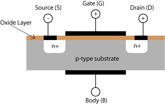
Read it in two directions:
- Vertically, the central stack is gate, insulating oxide, then silicon.
- Horizontally, the source and drain lie on opposite sides of the region beneath the gate.
The large gray region is the p-type substrate, also called the body. It is the starting silicon material surrounding the active parts of this transistor. The body contact shown underneath is useful context, but the five features to identify are the source, drain, channel, gate, and insulating layer.
| Feature | Where to find it in the cross-section | Core role |
|---|---|---|
| Source | One of the two heavily doped regions, at the left in this drawing | Supplies electrons to the conducting path in normal NMOS operation |
| Drain | The other heavily doped region, at the right in this drawing | Collects electrons from that path |
| Channel | The narrow silicon region under the oxide and between source and drain | The controllable path that can connect source and drain |
| Gate | The conductive electrode above the oxide | Uses an electric field to control the channel |
| Insulating layer | The thin oxide layer directly between gate and silicon | Electrically isolates the gate while allowing its electric field to affect the silicon |
The notation means heavily doped n-type silicon. These regions have many mobile electrons and are designed to make good electrical contact with the channel when the transistor is turned on.
The gate is close to the silicon—but not connected to it
The most distinctive feature of a MOSFET is the thin insulating layer between gate and silicon. In the diagram, it is the orange oxide layer. It is commonly silicon dioxide, , though real manufacturing technologies can use more complex insulating stacks.
Because the oxide is an insulator, an ideal gate does not conduct a direct DC current into the silicon. Instead, a voltage on the gate establishes an electric field through the thin oxide. That field changes the distribution of charge in the silicon immediately below.
This geometry is why the gate must be identified carefully:
- The gate is the black conductive feature on top.
- The oxide is the thin layer immediately beneath it.
- The channel is not the oxide and not the gate. It is in the silicon just below the oxide.
The three-dimensional view makes this spatial arrangement clearer. The gate extends across the gap between the source and drain, with its oxide insulation beneath it.
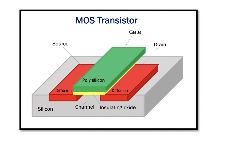
The red source and drain regions may look structurally identical because, at the physical-layout level, they often are very similar. In a circuit, the applied voltages and carrier flow establish which side functions as the source and which as the drain. In this simplified NMOS illustration, the left side is designated source and the right side drain.
The channel is a controlled region of silicon
The channel is the most easily misunderstood part because, in an enhancement-mode NMOS transistor, it is not a separately deposited wire or a permanently visible strip of material.
It is the region:
- between the source and drain,
- directly underneath the gate oxide, and
- within the p-type silicon surface.
With no sufficient positive voltage at the gate, the p-type silicon between the two regions does not provide a continuous electron-conducting path. The source and drain are therefore effectively isolated.
When the gate becomes sufficiently positive relative to the source and body, its electric field attracts electrons toward the silicon surface below the oxide and pushes holes away. If enough electrons accumulate, this surface region becomes n-type in behavior and forms a continuous conducting channel between source and drain.
Watch “How Does a MOSFET Work?” by Explorer for a visual construction of the NMOS structure, followed by an animation of the channel forming under the oxide.
First watch the physical structure, identifying the substrate, source, drain, insulating barrier, and gate. Then watch channel formation. Focus on the fact that electrons gather beneath the insulating layer rather than crossing through it into the gate.
This distinction is central:
- Channel region means the location under the gate between source and drain.
- Conducting channel means that this region currently contains enough mobile carriers to connect source and drain.
For the enhancement-mode NMOS shown here, a conducting channel exists only when the gate voltage exceeds a required level called the threshold voltage. Later, when we study transistor fabrication, this will help explain why precisely controlling oxide thickness, dopant placement, and gate dimensions matters so much.
Metal Oxide Semiconductor Field Effect Transistor (MOSFET)
Read DoITPoMS’ concise structural explanation of the MOSFET, then its account of how a positive gate voltage creates the conducting channel. It connects the visual labels in the diagram to the device’s basic switching behavior.
Under the page heading “Metal Oxide Semiconductor Field Effect Transistor (MOSFET),” read the complete opening structural paragraph, beginning with the description of the p-type substrate and the embedded source and drain regions. Pay particular attention to the physical stack: source and drain contacts, oxide film, gate electrode, and body. Then continue with the following explanation of switching operation, beginning at “Since the gate electrode is positively charged” and ending when the channel permits current flow. Focus on channel creation immediately below the oxide.
A reliable method for identifying the five features
When looking at a new simplified MOSFET cross-section, use this sequence:
-
Find the gate first. It is the conductor above the silicon surface, usually a horizontal strip extending over the central region.
-
Locate the insulating layer directly below the gate. It is thin and lies between gate and semiconductor. In simplified diagrams it is usually explicitly labeled oxide.
-
Identify the source and drain. Look for the two doped regions on either side of the gate. In an NMOS cross-section, they are generally n-type regions within p-type silicon.
-
Mark the channel location. It occupies the silicon surface under the gate oxide, stretching across the gap between the inner edges of source and drain.
-
Keep the physical path separate from the electrical control. Source and drain carry the main current when the transistor is on; the gate controls that path through an electric field across the insulating layer.
A compact verbal description of the diagram is:
Two source and drain regions sit in a p-type silicon substrate. A gate electrode lies above the gap between them, separated from the silicon by a thin insulating oxide. The channel forms in the silicon surface beneath that oxide.
That sentence captures the physical relationship that later fabrication steps must create.
Common identification errors
A few mistakes are worth eliminating early.
| Mistake | Correction |
|---|---|
| Calling the oxide layer the channel | The oxide is an insulator. The channel is in the silicon below it. |
| Treating the gate as directly wired to the silicon | The gate is electrically isolated by the insulating layer; it controls silicon through an electric field. |
| Looking for a permanent channel strip in an enhancement NMOS | The channel is induced by a sufficient gate voltage. At zero gate bias, it is not a continuous conducting path. |
| Assuming “source” always means the left side | The drawing convention may place it on either side. Its circuit function and applied voltages determine the designation. |
| Calling all silicon below the gate “the channel” | More precisely, the channel is the near-surface region directly under the oxide and between source and drain. |
For this course, the simplified NMOS geometry is the reference picture. Real chips contain enormous numbers of related transistor structures, with much smaller dimensions and more elaborate material stacks, but the same essential gate–insulator–silicon relationship remains fundamental.
Key takeaways
A simplified NMOS MOSFET can be read as a controllable bridge built into silicon:
- The source and drain are the two doped semiconductor regions on opposite sides of the device.
- The channel is the silicon region between them, directly beneath the insulating layer.
- The gate is the conductive electrode above the channel region.
- The insulating layer, commonly an oxide, separates the gate from silicon while allowing the gate’s electric field to control the channel.
- A sufficiently positive NMOS gate voltage creates a conducting electron channel, allowing current to pass between source and drain.
You have now reached the basic device structure that fabrication is designed to build. In the next module, we begin the fabrication toolkit itself with deposition: the processes used to add the thin insulating, conducting, and semiconducting films from which structures such as the gate stack are made.