Recommended resources
The freely available resources this lesson will direct you to.
- ‘Semiconductor Manufacturing Process’ Explained | 'All About Semiconductor' by Samsung Semiconductorwww.youtube.com
- How are Microchips Made? 🖥️🛠️ CPU Manufacturing Process Stepswww.youtube.com
- What is ASIC Design? – How it Workswww.synopsys.com
- 6 crucial steps in semiconductor manufacturingwww.asml.com
Welcome to Chip Technology. This first module follows the full path of an integrated circuit: an idea expressed as a circuit design becomes many physical copies on a silicon wafer, then becomes a protected, testable component ready for a system.
By the end of this lesson, you should be able to narrate that journey in the right order and, more importantly, explain what changes at each major handoff: from a design description to manufacturing data, from a wafer to individual dies, and from a bare die to a qualified packaged chip.
A useful distinction from the start: the word chip can mean either the tiny piece of silicon, called a die, or the familiar black, metal-topped, or ball-grid packaged component. The silicon die is made during wafer fabrication; the finished component exists only after assembly, packaging, and final test.
1. Before silicon: defining and proving the circuit
A fab cannot manufacture an idea directly. First, engineers must turn a desired product into an exact, testable physical description.
For a digital chip, work commonly begins with a specification: what the chip must do, how quickly it must operate, how much power it may consume, what it communicates with, how much area it may occupy, and what it costs to make. Architects divide that problem into functional blocks, such as processor cores, memory, graphics, communications, or control logic.
Design engineers then write a logical description of the circuit, often using a hardware description language. This describes circuit behavior rather than the final physical shapes of transistors and wires. Verification is crucial here: discovering a functional error before manufacturing is far less costly than discovering it after thousands of wafers have been processed.
What is ASIC Design? – How it Works
Read Synopsys’s overview of the ASIC design flow. It gives the essential bridge between a product requirement and the manufacturing data delivered to a foundry.
In the section “How Does ASIC Design Work?”, read all five numbered stages. Begin with specification and architecture, then follow RTL design and verification. Continue through physical implementation, and finish with tape-out and fabrication. Focus on how each stage makes the design more concrete and more physically constrained.
The key transition is called tape-out. It does not mean a physical roll of tape is sent to a factory. It means that the completed design is released as manufacturing data, including the geometric patterns for the many layers that will be formed on the wafer. A foundry uses this data to create masks or reticles for lithography and to configure its manufacturing flow.
Modern chips are also deliberately made testable. Design for test, often abbreviated DFT, adds structures that allow manufacturing test equipment to control and observe internal parts of a complex circuit. This is one of the links between pre-silicon design and the testing stages at the end of the journey.
At this point, the circuit exists as validated data. Nothing electronic has been built yet.
2. Fabrication: making many copies on one wafer
Manufacturing begins with a circular silicon wafer. The wafer serves as a shared platform for many copies of the same design. A large processor wafer may carry hundreds of dies; a smaller memory die may fit in much larger numbers. All of these dies are fabricated in parallel, layer by layer.
The simplified illustration below captures the broad journey. Treat it as a map rather than a literal one-pass recipe: deposition, lithography, etching, implantation, cleaning, measurement, and polishing recur many times as the three-dimensional circuit is constructed.
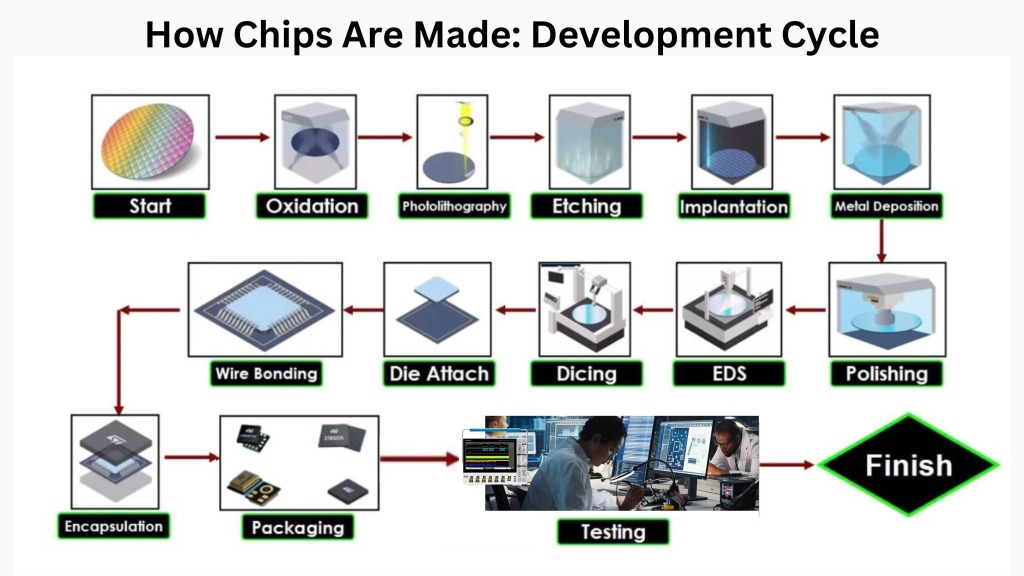
A wafer moves through a clean manufacturing environment and many specialized tools. At a high level, fabrication uses a repeated set of actions:
- Add or grow a layer. The added material might insulate electrically, conduct electricity, or alter the behavior of silicon.
- Apply a light-sensitive material called photoresist.
- Use lithography to place a layer-specific pattern onto the resist.
- Remove selected material by etching so the pattern becomes a physical feature.
- Modify selected regions, for example with implanted dopant ions, where transistor behavior must be controlled.
- Clean, inspect, and flatten the surface when needed before the next layer.
The lower region of the finished die contains the microscopic transistor structures that perform switching. Above them are many patterned layers of metal wiring separated by insulating material. Vertical connections link wiring layers so that billions of transistors can work as one circuit. Later lessons will examine these fabrication operations individually; for now, the important point is that chipmaking is controlled layered construction, not the carving of a circuit from a finished block.
‘Semiconductor Manufacturing Process’ Explained | 'All About Semiconductor' by Samsung Semiconductor
Watch “‘Semiconductor Manufacturing Process’ Explained” by Samsung Semiconductor Newsroom for a visual overview of the wafer-to-package portion of the journey. It is useful here because it keeps the major manufacturing stages in one continuous story.
Watch the overview to establish the main vocabulary. Then watch wafer preparation for the wafer and oxidation stages. Continue with patterning and wiring, paying attention to the recurring roles of photoresist, lithography, etching, deposition, and implantation. Finish with test and packaging. Focus on the distinction between building the die on the wafer and turning that die into a usable component.
The video’s sequence is deliberately simplified. For example, deposition is not a single event near the beginning: thin films are deposited many times, and the order depends on the layer being built. Likewise, an image may show “metal deposition” as one box, but functional metal interconnects require patterned lines, vertical connections, insulating layers, and repeated planarization.
This is why a completed wafer represents an enormous amount of work. It is not simply silicon with a drawing printed on top. It contains a dense, aligned stack of patterned materials, each made within tight dimensional and electrical tolerances.
3. Testing the wafer before it is cut
Once fabrication is complete, the wafer still holds all dies in their original grid. Before spending money to separate and package them, manufacturers test them on the wafer.
Tiny probes contact test pads on each die. Automated equipment applies electrical signals, measures responses, and identifies failures. This is commonly called wafer test, wafer probe, or electrical die sort. In the development-cycle illustration, it appears as EDS.
This step has two practical purposes:
- It prevents clearly defective dies from being packaged.
- It classifies working dies by measured characteristics, such as operating speed, power consumption, or enabled functions.
The second purpose is called binning. A die that is functional but does not meet the most demanding speed or power target may still be valuable in a lower-tier product, provided it meets that product’s specification. Exact binning practices depend on the chip and manufacturer, but the broad principle is that testing helps match each die to an appropriate product category.
A wafer test is not the final verdict. At this stage, the die is exposed silicon with temporary electrical contact points. It has not yet been connected to a computer board, protected from its environment, or tested as a complete packaged product.
4. From a bare die to a finished component
After wafer test, a saw or laser separates the wafer into individual dies, a process called dicing. Good dies proceed to assembly and packaging, which provide three things a bare die lacks:
| Packaging function | Why it matters |
|---|---|
| Electrical connection | Routes the die’s tiny connection pads to larger package contacts that a circuit board can use. |
| Mechanical and environmental protection | Protects fragile silicon and delicate connections from damage, moisture, and contamination. |
| Thermal management | Helps move heat away from a working die. |
A die is mounted onto a package substrate, lead frame, or interposer, depending on the package type. Its contacts are connected to the package using methods such as wire bonding or flip-chip bonding. The assembly is then enclosed, often with molded encapsulation and, for higher-power devices such as processors, a heat spreader.
The packaged part undergoes final test. Test systems check that it works electrically in its intended package, meets relevant performance limits, and survives applicable handling or environmental screening. A chip is ready to ship only after it passes this stage.
How are Microchips Made? 🖥️🛠️ CPU Manufacturing Process Steps
Watch the final segment of Branch Education’s “How are Microchips Made?” for a compact walkthrough of post-fabrication decisions: wafer-level testing, sorting, dicing, assembly, cooling, and final checking.
Watch the post-fab journey. Notice that testing happens before the wafer is cut, that dies can be classified by their measured capability, and that the package includes both electrical routing and thermal hardware.
It is also useful to separate the die from the package in everyday language:
- A die is the fabricated piece of silicon cut from the wafer.
- A package is the structure that supports, protects, cools, and connects one or more dies.
- A chip product is the tested, specified component sold to a system maker or consumer.
Some modern products package multiple dies together, but the same broad journey remains: design, fabricate on wafers, test, separate or assemble dies, package, and test the finished unit.
The whole journey in one narrative
A team starts with requirements and produces an architecture. Engineers create and verify a detailed circuit description, translate it into a physical layout, add test features, and release manufacturing data at tape-out. A foundry uses that data to build many copies of the design simultaneously on silicon wafers through repeated layer-formation and patterning processes.
The completed wafer is electrically tested die by die. Usable dies are identified, the wafer is diced, and suitable dies are assembled into packages that provide external connections, physical protection, and heat removal. Final testing confirms that each packaged component meets its product specification.
The central idea to retain is this: design defines what should be built; fabrication builds it repeatedly on a wafer; packaging makes each die usable in the outside world; testing connects all three stages to product quality.
Next, we will look closely at the wafer itself and explain why chip fabrication begins with ultrapure, single-crystal silicon rather than ordinary silicon or a less controlled material.