Hello! Welcome back to our course on computational structures.
In our last lesson, we constructed a CMOS inverter and analyzed its voltage transfer characteristic (VTC). We saw how a complementary pair of pMOS and nMOS transistors creates a robust inverter with low static power consumption. This inverter forms the basis of all CMOS logic.
Today, we'll expand on that foundation to build more complex logic gates. The goal of this lesson is to learn how to apply the CMOS recipe to design NAND and NOR gates. You'll discover a systematic method for translating a Boolean logic function into a transistor-level circuit diagram, a fundamental skill for digital circuit design.
1. The CMOS Recipe
In the inverter, a single nMOS transistor formed the pull-down network (PDN) and a single pMOS formed the pull-up network (PUN). To create more complex functions, we will build more complex networks using transistors in series and parallel. The general structure remains the same:
- A pull-down network (PDN) made exclusively of nMOS transistors connects the output to Ground (logic '0').
- A pull-up network (PUN) made exclusively of pMOS transistors connects the output to Vdd (logic '1').
- For any valid input combination, only one network is active at a time. The PUN and PDN are complementary or dual networks.
The core of the design process, or the "CMOS recipe," is figuring out how to arrange the transistors in these networks. The key is to first focus on the pull-down network.
The Pull-Down Network (nMOS)
The PDN's job is to pull the output to '0'. Therefore, we design it to be ON for the input combinations that should produce a '0' at the output. Since nMOS transistors turn ON when their gate input is HIGH (logic '1'), we can use them to represent the variables in our logic function directly. The connections follow two simple rules:
- AND logic is implemented with nMOS transistors in series. The path to ground is only complete if ALL inputs are HIGH.
- OR logic is implemented with nMOS transistors in parallel. The path to ground is complete if ANY input is HIGH.
The Pull-Up Network (pMOS) and Duality
The PUN must be the complement of the PDN. It should be ON when the PDN is OFF, and vice-versa. This is achieved by creating a dual topology.
- If the PDN has transistors in series, the PUN will have corresponding pMOS transistors in parallel.
- If the PDN has transistors in parallel, the PUN will have corresponding pMOS transistors in series.
This powerful principle of duality stems from De Morgan's laws. Let's see how it works in practice.
6. CMOS - Computation Structures
The following course notes from computationstructures.org formalize this design process as the 'CMOS Gate Recipe.' It's a concise guide that we will be applying throughout this lesson.
Please read the section titled '6.3. The CMOS Gate Recipe'. Focus on the two main bullet points for designing a gate: either start with the pulldown circuit (for F=0) or the pullup circuit (for F=1), and then derive the complement.
2. Designing a 2-Input CMOS NAND Gate
Let's apply the recipe to a 2-input NAND gate. The Boolean expression is .
-
Design the Pull-Down Network (PDN):
- First, ask: When should the output be '0'? According to the truth table for NAND, only when A=1 AND B=1.
- The logic is an AND function.
- Therefore, we connect two nMOS transistors in series between the output and ground. One is controlled by input A, the other by input B.
-
Design the Pull-Up Network (PUN):
- The PUN is the dual of the PDN.
- The series nMOS network becomes a parallel pMOS network.
- We connect two pMOS transistors in parallel between Vdd and the output.
-
Combine and Verify:
The final circuit looks like this:
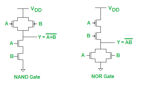
Let's trace the logic for the NAND gate:
- If A=1 and B=1, both nMOS transistors are ON, creating a path to ground. Both pMOS transistors are OFF. The output is 0.
- If either A=0 or B=0 (or both), at least one of the nMOS transistors is OFF, breaking the path to ground. At the same time, at least one of the pMOS transistors is ON, creating a path to Vdd. The output is 1.
The circuit works exactly as a NAND gate should.
To see this process animated and explained, please review the following resources.
6. CMOS - Computation Structures
The course notes we looked at earlier also provide a clear, step-by-step derivation of the 2-input NAND gate.
In the webpage, find section '6.3.1. Common 2-input gates' and read the subsection for the 'NAND gate'. Focus on how the truth table leads directly to the design of the series pulldown circuit.
CMOS Logic Gates Explained | Logic Gate Implementation using CMOS logic
To visualize the construction and operation, this video from ALL ABOUT ELECTRONICS is very helpful.
Watch the segment from 16:00 to 18:58. This part walks through the NAND gate implementation, showing the series nMOS and parallel pMOS networks and verifying the truth table.
3. Designing a 2-Input CMOS NOR Gate
Now let's design a 2-input NOR gate: .
-
Design the Pull-Down Network (PDN):
- When should be '0'? When A=1 OR B=1.
- The logic is an OR function.
- Therefore, we connect two nMOS transistors in parallel.
-
Design the Pull-Up Network (PUN):
- The dual of a parallel network is a series network.
- We connect two pMOS transistors in series.
-
Combine and Verify:
You can see the resulting circuit in the right-hand side of the "2-input CMOS NAND and NOR gates" image shown earlier. Let's trace it:
- If A=0 and B=0, both pMOS transistors are ON, creating a path to Vdd. Both nMOS transistors are OFF. The output is 1.
- If either A=1 or B=1 (or both), at least one of the pMOS transistors is OFF, breaking the series path to Vdd. At the same time, at least one of the nMOS transistors is ON, creating a path to ground. The output is 0.
This correctly implements the NOR function.

The following resources walk through the NOR gate design, reinforcing the recipe.
6. CMOS - Computation Structures
Now, let's look at the formal explanation for the NOR gate from the course notes.
Directly following the NAND gate section, read the part about the 'NOR gate'. Notice how the pulldown network now uses a parallel structure to implement the 'OR' condition for a zero output.
CMOS Logic Gates Explained | Logic Gate Implementation using CMOS logic
The same video also covers the NOR gate, which will help solidify your understanding of the duality principle.
Watch from 19:37 to 20:43. Observe how the parallel nMOS network corresponds to the NOR function's condition for a low output.
4. Practice Problem: A Complex Gate
Now that you have the recipe, let's apply it to a slightly more complex function, which is a great way to prepare for exam-style problems.
Consider the function:
Before watching the solution, try to design the pull-down network yourself:
- The output Z is '0' when .
- This means Z is '0' if OR if ( AND ).
- How would you combine series and parallel nMOS transistors to implement this?
Think about it for a moment...
The "OR" suggests a parallel structure. The "AND" suggests a series structure. So, you would have an nMOS transistor for input A in parallel with a series combination of two nMOS transistors for inputs B and C.
Now, what would the dual pull-up network look like?
Let's watch a worked example from MIT OpenCourseWare that solves a very similar problem. The video uses the function , which is exactly the one we just analyzed.
3.2.8 Worked Examples: CMOS Logic Gates
This video from MIT OpenCourseWare walks through designing a gate for the function Z = NOT(A OR (B AND C)). See how your own design matches up with their solution.
Watch the entire video (it's short, under 3 minutes). Pay close attention to how the Boolean expression is translated first into the n-FET pulldown network (00:50) and then how the dual p-FET pull-up network is derived from it (01:45).
Conclusion
In this lesson, you've learned the systematic CMOS recipe for designing logic gates. This method allows you to take any inverting Boolean function and translate it into a transistor-level circuit.
Key Takeaways:
- CMOS gates consist of a pull-down network (PDN) of nMOS transistors and a complementary pull-up network (PUN) of pMOS transistors.
- The design process starts with the PDN: implement the logic for when the output should be '0' using series (AND) and parallel (OR) nMOS transistors.
- The PUN is the dual of the PDN: series connections become parallel, and parallel connections become series.
- A NAND gate uses series nMOS (PDN) and parallel pMOS (PUN).
- A NOR gate uses parallel nMOS (PDN) and series pMOS (PUN).
Preview of the Next Lesson
Now that we know how to build these gates, we need to analyze how fast they operate. In the next lesson, we will define and calculate propagation delay and contamination delay for a CMOS gate. These are critical timing parameters that determine the maximum speed of any digital circuit.