Hello! Welcome back to our course on computational structures.
In the last lesson, we established the fundamental building blocks of modern digital circuits: nMOS and pMOS transistors, which act as complementary voltage-controlled switches. We saw that nMOS is great for pulling an output down to '0' (GND) and pMOS is great for pulling it up to '1' (Vdd).
Today, we will combine these two components to build the simplest and most fundamental logic gate: the CMOS inverter. Our learning outcome is to construct a CMOS inverter and trace its Voltage Transfer Characteristic (VTC). This lesson is crucial as it bridges the gap between the physical behavior of transistors and the abstract digital logic levels we discussed earlier.
1. Constructing the CMOS Inverter
The goal of an inverter is to output a HIGH voltage when the input is LOW, and a LOW voltage when the input is HIGH. Based on our last lesson, this suggests a clear strategy:
- When the input is LOW (Logic '0'), we want to connect the output to Vdd. The pMOS transistor turns ON with a LOW input, making it the perfect candidate for this job (a "pull-up" device).
- When the input is HIGH (Logic '1'), we want to connect the output to GND. The nMOS transistor turns ON with a HIGH input, making it ideal for this task (a "pull-down" device).
By combining a pMOS pull-up network and an nMOS pull-down network, we get a Complementary Metal-Oxide-Semiconductor (CMOS) inverter.
The video below first recaps why nMOS and pMOS are not good at passing weak logic levels (a concept from our last lesson) and then shows exactly how they are combined to form a robust inverter that produces strong '0's and '1's.
Inverter - 1 - CMOS Inverter Construction
This video from NPTEL-NOC IITM explains why we need both transistor types and then demonstrates how to construct a CMOS inverter.
Please watch the segment from 04:09 to 24:14. Pay close attention to: Why an nMOS transistor alone struggles to charge a capacitor to Vdd (04:09 - 13:32). Why a pMOS transistor alone struggles to discharge a capacitor to ground (13:32 - 18:32). How connecting them in a complementary fashion solves these issues and creates a natural inverter (18:32 - 24:14).
As the video explained, the standard CMOS inverter is constructed as follows:
- The pMOS transistor's source is connected to the power supply, Vdd.
- The nMOS transistor's source is connected to Ground (GND).
- The drains of both transistors are connected together. This connection point is the inverter's output (Vout).
- The gates of both transistors are connected together. This forms the inverter's input (Vin).
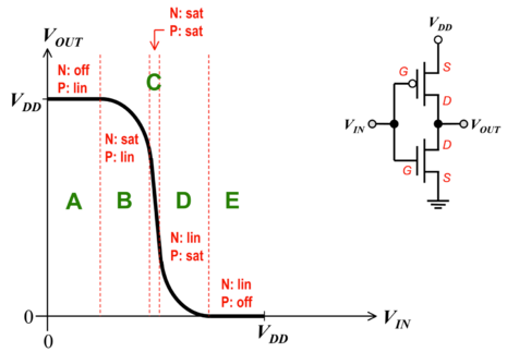
This simple, elegant structure is the heart of CMOS technology. Notice that for any static input (either a stable '0' or a stable '1'), one transistor is ON while the other is OFF. This prevents a direct path from Vdd to GND, which is why CMOS logic has very low static power consumption.
2. Tracing the Voltage Transfer Characteristic (VTC)
The VTC plots the output voltage (Vout) as a function of the input voltage (Vin). While we know the output for Vin=0 and Vin=Vdd, the VTC shows us what happens for all voltages in between. This curve tells us everything about the inverter's static behavior, including its logic levels and noise margins.
To trace the VTC, we imagine slowly sweeping the input voltage Vin from 0V all the way to Vdd and observing the corresponding Vout. As Vin changes, the operating modes of the nMOS and pMOS transistors (cutoff, linear, saturation) will change, defining distinct regions of the VTC.
The following video provides an excellent intuitive and analytical walkthrough of this process.
Inverter - 2 - Voltage Transfer Characteristics
This follow-up video explains how the VTC is derived by analyzing the currents and operating regions of the two transistors as the input voltage sweeps from 0 to Vdd.
Watch the segment from 02:32 to 20:12. Focus on: The fundamental constraint that the drain currents of the nMOS and pMOS must be equal in magnitude (02:32 - 07:36). The intuitive walkthrough of the five distinct operating regions of the VTC as Vin increases (09:41 - 18:15). The comparison between the real VTC and an ideal, perfectly sharp VTC (18:31 - 20:12).
3. The Five Regions of the VTC
As you saw in the video and the image above, the VTC is divided into five regions based on the state of the two transistors. Let's summarize them. (Here, is the positive threshold voltage of the nMOS, and is the negative threshold voltage of the pMOS).
-
Region A:
Vinis low (0 ≤Vin< )- nMOS: OFF (in cutoff), since
Vinis below its threshold. It acts like an open switch. - pMOS: ON (in linear/ohmic region), since its gate voltage is far below its source voltage. It acts like a low-resistance path to Vdd.
- Result: The output
Voutis pulled up to Vdd.
- nMOS: OFF (in cutoff), since
-
Region B:
Vinis rising (V_{tn}≤Vin<Vout+ )- nMOS: Turns ON (in saturation), as it now has enough gate voltage to conduct, and its drain voltage (
Vout) is high. - pMOS: Remains ON (in linear region).
- Result: The nMOS starts to pull the output down.
Voutbegins to drop from Vdd.
- nMOS: Turns ON (in saturation), as it now has enough gate voltage to conduct, and its drain voltage (
-
Region C:
Vinis near the switching threshold- nMOS: ON (in saturation).
- pMOS: ON (in saturation).
- Result: Both transistors are strongly conducting. This is the region of highest gain, where a tiny change in
Vincauses a large change inVout. The VTC curve is nearly vertical here. The point whereVin=Voutis called the switching threshold, .
-
Region D:
Vinis high (Vout+ <Vin≤ Vdd + )- nMOS: ON (in linear region), because its drain voltage (
Vout) has now dropped significantly. - pMOS: ON (in saturation), as its gate voltage is still low enough relative to its source to keep it saturated.
- Result:
Voutcontinues to fall towards GND.
- nMOS: ON (in linear region), because its drain voltage (
-
Region E:
Vinis very high (Vin> Vdd + )- nMOS: ON (in linear region), acting like a low-resistance path to GND.
- pMOS: OFF (in cutoff), because the gate voltage
Vinis now too high. - Result: The output
Voutis pulled down to GND (0V).
For a more detailed mathematical treatment, which may be useful for solving exam problems, the following resource breaks down the current equations for each of the five regions.
This tutorial page provides a step-by-step derivation of the VTC, including the specific equations for drain current in each of the five operating regions.
Read the section titled 'The VTC of complementary CMOS inverter is as shown in above Figure'. Focus on understanding which transistor is in which mode (linear, saturation, cutoff) in each region and the corresponding current equations. This level of detail is excellent for exam preparation.
Conclusion
Today we connected the dots from individual transistors to a functional logic gate. You have learned how to build the most fundamental element of digital logic and how to characterize its behavior.
Key Takeaways:
- A CMOS inverter is constructed from a pMOS pull-up network and an nMOS pull-down network.
- This complementary design ensures a rail-to-rail output swing (from 0 to Vdd) and low static power consumption.
- The Voltage Transfer Characteristic (VTC) describes the inverter's output for any given input.
- The VTC is shaped by the five distinct operating regions, determined by the combination of cutoff, linear, and saturation states of the nMOS and pMOS transistors.
Preview of the Next Lesson
We have successfully built a NOT gate. But how do we build more complex logic like NAND and NOR? In the next lesson, we will apply the CMOS recipe to design NAND and NOR gates. You will see that the same principle of a pMOS pull-up network and an nMOS pull-down network applies, but we will use series and parallel combinations of transistors to implement the desired logic function.