Hello! Let's dive into the final lesson of our first module on the digital abstraction and CMOS logic.
In our previous session, we mastered the "CMOS recipe," learning how to construct fundamental logic gates like NAND and NOR, as well as more complex ones, by combining nMOS and pMOS transistors into pull-up and pull-down networks. We now have the building blocks of a digital system.
However, just building them isn't enough. For a digital system to work correctly, it must also be fast enough. This brings us to the crucial topic of timing. Gates don't respond instantly. This lesson will focus on characterizing this delay. Our goal is to define and calculate propagation delay and contamination delay for a CMOS gate. Understanding these two parameters is fundamental to analyzing the performance and correctness of any digital circuit.
1. The Physical Origin of Delay
Why isn't a logic gate's output instantaneous? The answer lies in the physics of the circuit. As an electrical engineering student, you know that any physical wire has resistance and capacitance. In a CMOS circuit, the output of a gate is connected to the inputs of other gates. These connections, along with the transistor gates themselves, create a load capacitance (C_load).
When the input to a gate changes, the pull-up or pull-down network must charge or discharge this C_load. This process isn't instant; it's governed by the RC time constant, where R is the effective resistance of the 'ON' transistors in the network.
- Output going from HIGH to LOW: The pull-down network turns ON, discharging
C_loadto ground through the nMOS transistors. - Output going from LOW to HIGH: The pull-up network turns ON, charging
C_loadfrom Vdd through the pMOS transistors.
This charging and discharging process is the physical source of delay in CMOS logic.
Propagation Delay of CMOS Inverter | Minimization of Propagation Delay of CMOS Inverter
To start, let's watch a video from Engineering Funda that provides an excellent intuitive explanation of propagation delay in a CMOS inverter, connecting it directly to the charging and discharging of this load capacitance.
Watch the first part of the video, from the beginning to 05:43. Focus on how an input transition causes the pMOS or nMOS transistor to switch on, leading to a period of charging or discharging that results in a delayed output transition.
2. Propagation Delay (t_PD)
Now let's formalize this concept. The propagation delay (t_PD) is an upper bound on the time it takes for a gate's output to become valid and stable after its inputs have become valid. It's the "worst-case" delay; the manufacturer guarantees the gate will have settled to its correct new output value within this time.
Because the charging (pull-up) and discharging (pull-down) paths can have different effective resistances, we distinguish between two types of propagation delay:
t_PLH: The delay for the output transitioning from Low to High.t_PHL: The delay for the output transitioning from High to Low.
The overall propagation delay t_PD for the gate is the maximum of these two: .
There are two common ways to measure this delay on a voltage waveform:
- From 50% to 50%: A common engineering simplification is to measure the delay from the time the input signal crosses 50% of Vdd to the time the output signal crosses 50% of Vdd.
- Using Logic Thresholds: A more rigorous definition, which connects to our digital abstraction, measures the delay from when the input becomes a valid logic level (crossing
V_IHorV_IL) to when the output becomes a valid logic level (crossingV_OHorV_OL).
L03: CMOS Technology - Computation Structures
The following course notes from Computation Structures provide a clear, rigorous definition of propagation delay using the logic thresholds we learned about in the first lesson.
Please read the section that starts with the paragraph 'The propagation delay of a combinational logic gate is defined to be an upper bound on the delay from valid inputs to valid outputs.' Study the waveform diagram carefully to see how the delay is measured between the input crossing V_IH/V_IL and the output crossing V_OL/V_OH.
For a slightly different perspective that uses the 50% measurement point, you can review the lecture slides from UT Austin. They also introduce the common notations t_pdr (rising) and t_pdf (falling).
[PDF] 5. CMOS Gate Characteristics
These lecture notes provide the formal definitions for rising and falling propagation delays, as well as the average propagation delay.
On slide 19, titled 'Delay Definitions', look at the definitions for tpdr, tpdf, and tpd. Notice that these are measured from the input crossing VDD/2 to the output crossing VDD/2.
3. Contamination Delay (t_CD)
While t_PD tells us the longest we have to wait for the output to be correct, contamination delay (t_CD) tells us the shortest amount of time the output is guaranteed to remain at its old, stable value after the inputs start to change. It is a lower bound on the delay.
In other words, after an input transition, you can rely on the old output value for at least t_CD seconds. After that, the output is in an unknown state (it might be changing, or even glitching) until t_PD has passed.
The t_CD specification is crucial for preventing timing errors in sequential circuits, a topic we will cover in detail later in the course. If a data sheet doesn't specify a t_CD, you must make the conservative assumption that t_CD = 0, meaning the output could change instantaneously with the input.
L03: CMOS Technology - Computation Structures
Let's return to the Computation Structures notes to see the formal definition of contamination delay.
Read the sections beginning with 'Although not strictly required by the static discipline, it will be useful to define another timing specification, called the contamination delay' and 'So here’s a quick summary of the timing specifications for combinational logic.' Pay attention to the waveform diagram showing the measurement and the summary diagram illustrating the 'invalid' output region between t_CD and t_PD.
4. Calculating Delays in a Circuit
Now that we understand delays for a single gate, how do we find the total delay of a circuit made of many gates? The principle is straightforward:
- The overall
t_PDof a combinational circuit is determined by the longest path from any input to any output. This is called the critical path. You find it by summing thet_PDvalues of all gates along every possible path and taking the maximum sum. - The overall
t_CDof a circuit is determined by the shortest path from any input to any output. You find it by summing thet_CDvalues of gates along every path and taking the minimum sum.
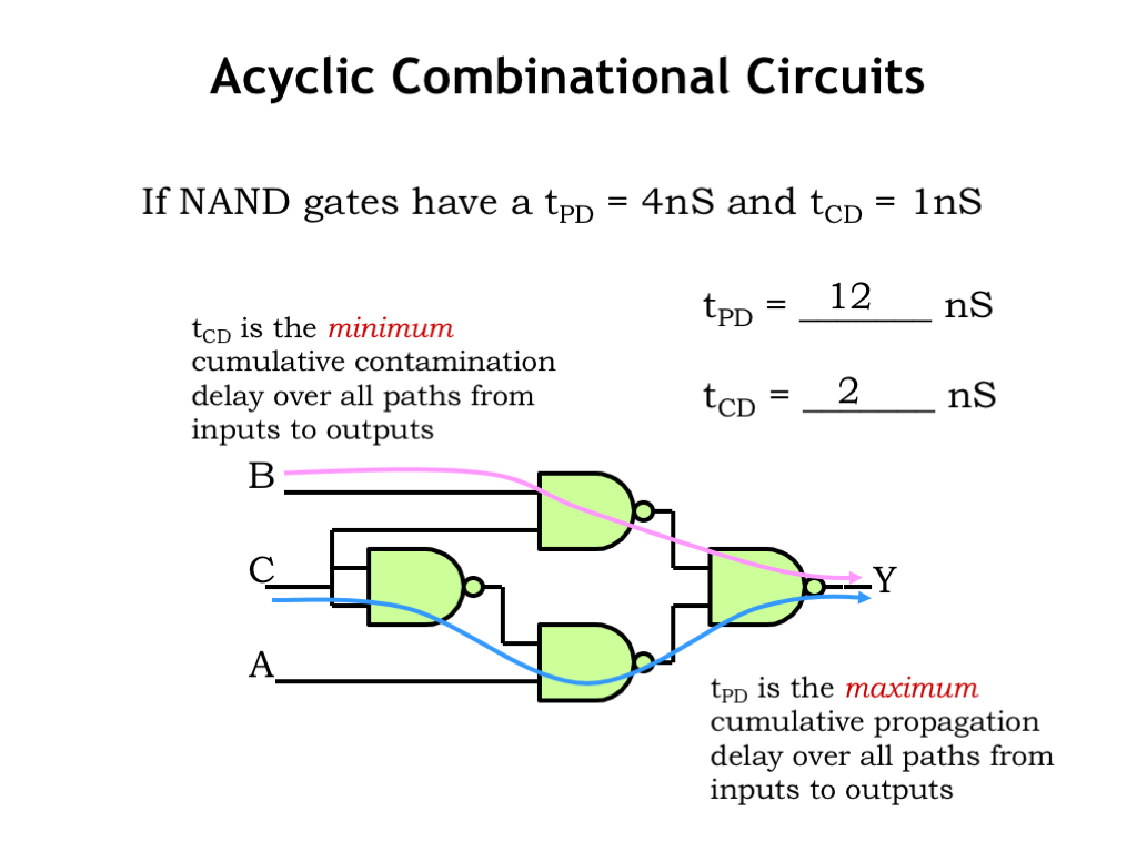
This process is fundamental to timing analysis. Let's read the formal explanation and then watch a video showing a quick method for doing this on a circuit diagram, which is a very useful skill for your exam.
L03: CMOS Technology - Computation Structures
The Computation Structures notes explain this path-based calculation method using the exact circuit shown in the image above.
Read the final section, 'How do we calculate the propagation and contamination delays of a larger combinational circuit from the timing specifications of its components?'. Follow the logic for finding the 12 ns propagation delay and the 2 ns contamination delay.
Digital Design (120 8a3) Propagation Delays 1 (gate-level circuits)
This video demonstrates a very practical and quick way to calculate the overall propagation delay by annotating the delays directly onto the circuit diagram. This is an excellent technique for solving problems quickly.
Watch the segment from 08:56 to 10:54, titled 'A quicker way'. Observe how the presenter works from left to right, adding the gate delay to the largest input delay at each stage to find the final output delays.
5. A Deeper Look: Estimating Gate Delays
Where do the t_PD numbers for individual gates come from? As we discussed, they are based on the RC time constant. For a simple inverter, this is relatively easy to model. For more complex gates like NAND or NOR, the effective resistance R depends on the number of transistors in series.
For example, in the pull-down network of a 3-input NAND gate, the worst-case (slowest) discharge path is through all three nMOS transistors in series. The resistance of this path is roughly three times that of a single transistor, leading to a longer delay.

A more formal method for estimating the delay in such RC networks is the Elmore delay model. It provides an approximation by summing the resistance-capacitance products for each node in the path. While we won't do detailed Elmore calculations, it's valuable to know that this is a technique used to derive the single t_PD value for a complex gate from its transistor-level structure.
[PDF] 5. CMOS Gate Characteristics
These lecture notes introduce the Elmore delay model. It's a powerful tool for estimating delays in RC ladder networks, which is what a series chain of MOSFETs looks like.
Skim slide 27 ('Elmore Delay') to understand the formula, which sums the resistance from the source to each node multiplied by the capacitance at that node. Then, look at the example on slides 30 and 31, which apply this model to estimate the rising and falling propagation delays of a 2-input NAND gate. The goal is to appreciate the method, not to memorize the formulas.
Conclusion
This lesson completes our first module by adding the critical dimension of time to our understanding of CMOS circuits. We've moved from the static behavior of logic gates to their dynamic performance.
Key Takeaways:
- Gate delays are caused by the time it takes to charge and discharge the load capacitance through the resistance of the MOSFETs.
- Propagation Delay (
t_PD) is an upper bound on delay. It tells you the maximum time you must wait for a gate's output to be stable and correct after an input change. - Contamination Delay (
t_CD) is a lower bound on delay. It guarantees the minimum time a gate's previous output will remain valid after an input change. - In a circuit, the overall
t_PDis the delay of the longest (critical) path, while the overallt_CDis the delay of the shortest path.
Preview of the Next Lesson
We have now fully covered the fundamentals of the digital abstraction and CMOS technology. In the next module, we will move up a level of abstraction. We will begin our study of Combinational Logic Synthesis and Optimization. The first step will be learning how to formally express any Boolean function using a truth table and derive its canonical sum-of-products (SOP) form, which is a universal way to describe any logic function.