Hello! In our last lesson, we saw how to use case statements to build combinational decoders in a clean and efficient way. We focused on making our design intent clear and preventing unintended latches.
Today, we'll continue building fundamental combinational blocks by tackling the N-bit adder. The key new concept we'll introduce is parameterization. You will learn how to write a single, flexible Verilog module for an adder that can be configured to any bit width—8 bits, 32 bits, 64 bits, and so on—without rewriting the code. This is a cornerstone of creating reusable and scalable digital designs, a critical skill for your upcoming bootcamp.
By the end of this lesson, you will be able to implement a fully parameterized N-bit adder in Verilog.
1. The Power of Parameters
In software, you might pass an argument to a function to change its behavior. In hardware design, we often need to define structural properties of a module before the design is synthesized—for example, the width of a data bus or the size of a memory. This is where Verilog's parameter keyword comes in.
A parameter is a constant value that is local to a module but can be overridden when that module is instantiated. This allows us to create generic, reusable "blueprint" modules.

By declaring parameter WIDTH = 8, we give our adder a default width of 8 bits. We can then use WIDTH throughout the module to define the size of our ports and internal signals. When we instantiate the module, we can either use the default 8-bit width or specify a new one, like adder #(32) my_32bit_adder (...).
2. Behavioral Modeling: The Direct Approach
Given your background in electronics, you know that adding two N-bit numbers can be done by cascading N full adders to create a ripple-carry adder. While we can model this structure directly in Verilog (as we'll see later), there's a much more straightforward and common way.
Verilog includes built-in arithmetic operators. The + operator is understood by synthesis tools, which can then infer the most efficient adder circuit for the target technology (be it an ASIC or an FPGA). This is called behavioral modeling—we describe what we want to do (add two numbers), not how to do it with gates.
Watch this video to see how a simple, parameterizable N-bit adder is coded and tested.
FPGA project 03 Part1 - Binary adder to 7 segment display
The "Ovisign Verilog HDL Tutorials" channel provides a clear walkthrough of designing and coding a parameterized N-bit adder.
Watch the following two segments: First, the project overview explains the core idea, paying special attention to why the output (sum) needs to be N+1 bits wide to accommodate the final carry. Next, review the Verilog code itself. Notice the parameter declaration and the simple sum = a + b line inside the always block.
As the video shows, the core logic can be as simple as sum = a + b. The synthesis tool handles the rest.
There are two common ways to handle the output of an adder:
- Combined Sum: As seen in the video, you can have a single output that is
N+1bits wide to hold both the N-bit sum and the 1-bit final carry.// N = 8 // input [7:0] a, b; // output [8:0] sum; // assign sum = a + b; - Separate Sum and Carry: It is often more convenient to have the N-bit sum and the 1-bit carry-out as separate ports. We can achieve this using Verilog's concatenation operator
{}.// N = 8 // input [7:0] a, b; // output [7:0] sum; // output cout; assign {cout, sum} = a + b;
In this second, very common pattern, the result of a + b (which is an N+1 bit value) is split. The most significant bit is assigned to cout, and the lower N bits are assigned to sum. This is the method we will use.
3. Structural Modeling: Building from the Ground Up with generate
While behavioral modeling is preferred for its simplicity and efficiency, it's also valuable to understand how you could construct an N-bit adder from smaller pieces. In Module 2, you learned that a 4-bit adder can be built by cascading four 1-bit full adders.
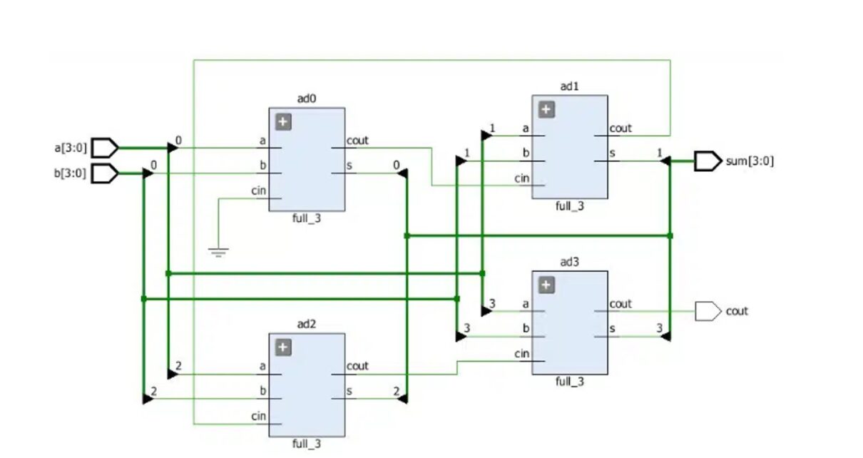
Instead of manually instantiating dozens of full adders, we can use a generate block to create repetitive structures programmatically. A generate for loop allows the synthesis tool to unroll the loop and create multiple instances of a module or logic block.
Combining Parameters and Generate Blocks
This document from MIT provides an excellent example of combining a parameter with a generate block to create a truly scalable ripple-carry adder.
Please study the slide titled "Combining parameters + generate blocks enables more powerful elaboration". Focus on how the parameter WIDTH is used to define the ports, the internal carry wire, and the bounds of the for loop inside the generate block. This demonstrates how a single piece of code can generate an adder of any size.
This structural approach gives you explicit control over the hardware structure, which can be useful in certain advanced designs. However, for a standard component like an adder, trusting the synthesis tool with a behavioral + operator is usually the best practice.
4. Your Turn: Implement a Parameterized Adder
Now, let's put this into practice. Your task is to write a Verilog module for a parameterized N-bit adder using the behavioral approach.
Specifications:
- Module Name:
adder_Nbit - Parameter:
WIDTH, with a default value of8. - Inputs:
[WIDTH-1:0] a: First N-bit input.[WIDTH-1:0] b: Second N-bit input.cin: 1-bit carry-in.
- Outputs:
[WIDTH-1:0] sum: N-bit sum output.cout: 1-bit carry-out.
- Implementation: Use a single continuous
assignstatement and the+operator. Remember to include thecinin your addition. Use the concatenation{}to assign tosumandcout.
Fill in the logic below:
module adder_Nbit #(
    parameter WIDTH = 8
) (
    input  [WIDTH-1:0] a,
    input  [WIDTH-1:0] b,
    input              cin,
    output [WIDTH-1:0] sum,
    output             cout
);

    // Your single line of code goes here

endmodule
Solution
module adder_Nbit #(
    parameter WIDTH = 8
) (
    input  [WIDTH-1:0] a,
    input  [WIDTH-1:0] b,
    input              cin,
    output [WIDTH-1:0] sum,
    output             cout
);

    // The result of a + b + cin is WIDTH+1 bits.
    // The MSB is assigned to cout, and the lower WIDTH bits are assigned to sum.
    assign {cout, sum} = a + b + cin;

endmodule
This compact and elegant line of code describes a fully functional and scalable N-bit adder. A synthesis tool can take this description and create an optimal hardware implementation, whether it's a simple 8-bit adder or a complex 64-bit one.
Conclusion
In this lesson, you have learned one of the most important concepts in modern RTL design: parameterization. By using parameter, you can create flexible, reusable modules that form the building blocks of larger systems.
Key Takeaways:
- Parameters make Verilog modules reusable and scalable by allowing you to configure properties like bit width during instantiation.
- For standard arithmetic like addition, behavioral modeling using the
+operator is the preferred, synthesis-friendly approach. It allows the tools to optimize the hardware for you. - The
{cout, sum}concatenation is a standard idiom for capturing the result and carry-out from an addition. generateblocks provide a powerful way to create repetitive hardware structures, such as a structural ripple-carry adder, by programmatically instantiating modules in a loop.
You have now completed the module on modeling combinational logic in Verilog! You can model multiplexers, decoders, and now, scalable adders.
In our next lesson, we will make a significant shift and begin our journey into sequential logic. We will start by modeling the fundamental unit of memory in digital circuits: the D-type flip-flop. This will open the door to designing circuits that have state and can perform operations over multiple clock cycles.