Hello! In our last lesson, we examined the standard cell library, the fundamental "parts catalog" of ASIC design. We saw how it provides different views of each cell—like the timing view (.lib) for synthesis and the physical view (.lef) for the tools that build the chip.
Today, we'll follow the design flow to that next step. We'll explore what happens after synthesis delivers its gate-level netlist. This is where the abstract list of gates and connections is transformed into a concrete, physical layout on silicon. This lesson will focus on two of the most critical stages in the entire ASIC flow: placement and routing.
Your learning goal is to describe what placement and routing accomplish in the physical design stage. By the end, you will understand how millions of individual components are arranged and interconnected to create a functional chip.
Let's begin by looking at where these steps fit in the larger process.

1. Placement: Arranging the Components
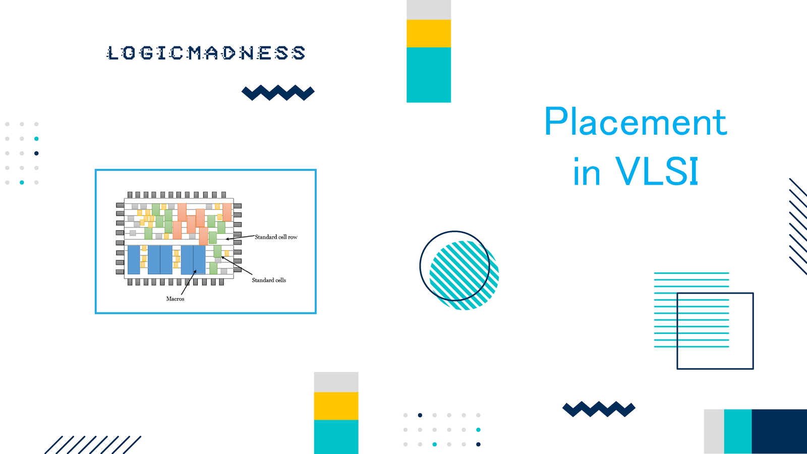
After synthesis, your design is a "netlist"—a massive text file describing millions of standard cells and how they're connected. It's like having a list of all the components for a city but with no map. Placement is the process that creates that map. Its primary job is to assign a specific physical location on the chip for every single standard cell.
Place and Route: Ultimate Guide
This section from AnySilicon's guide provides a clear and concise definition of placement and routing, outlining their primary goals.
Read the subsection titled "Definition and Purpose". Focus on the descriptions for both the placement and routing processes. Note the goals mentioned for each, such as minimizing delays for placement and avoiding signal interference for routing.
As the reading highlights, this isn't a random process. The placement tool, a sophisticated piece of software, works to achieve several competing goals simultaneously:
- Minimize wire length: Placing connected cells close together reduces the length of the wires needed, which in turn reduces signal delay and power consumption.
- Minimize routing congestion: If too many connections are needed in one small area, it becomes physically impossible to route all the wires. Good placement avoids creating these "congested" hotspots.
- Meet timing requirements: The tool uses your timing constraints (the SDC file) to prioritize placing cells on critical paths closer together to ensure the signals arrive on time.
To achieve this, the placement process is typically broken into a few key steps. The following video explains this progression from a rough-draft placement to a final, optimized layout.
Placement | Physical Design | Back To Basics
The "Placement" video from the Back To Basics channel details the sub-stages of placement, from an initial rough layout to the final legal and optimized arrangement.
First, watch the brief introduction to solidify the definition of placement. Next, watch the explanation of Global Placement. Pay attention to how the tool divides the area into "g-cells" and performs a rough placement that may have overlaps. This stage is about getting the big picture right. Finally, watch the section on Detailed Placement. This covers "legalization," which fixes the overlaps, and "optimization," the iterative process of fine-tuning the placement for better timing and power.
After these steps are complete, the abstract netlist now has a physical representation. Every standard cell has a coordinate on the chip, aligned in neat rows, ready to be wired up.
2. Routing: Making the Connections
With all the cells in their final positions, the next task is to physically connect them. Routing is the process that creates the metal wires between the cell pins, following the connections defined in the netlist. If placement was about creating the city map, routing is about building the roads, power lines, and communication cables.
The goals of routing are to:
- Complete all connections: The primary goal is to successfully route 100% of the nets.
- Adhere to design rules: The foundry provides a complex set of "Design Rules" that dictate the minimum width of wires and the minimum spacing between them. Violating these rules (a "Design Rule Check" or DRC violation) can make the chip unmanufacturable.
- Meet timing: The router must use shorter paths for critical signals to ensure the chip runs at the target speed.
Similar to placement, routing is a multi-step process that moves from high-level planning to fine-grained implementation.
Routing | Physical Design | Back To Basics
The "Routing" video, also from Back To Basics, explains the stages involved in creating the physical wire connections across the chip.
Start with the definition of routing to understand its core purpose. Then, watch the segment on Global Routing. Note the similarity to global placement; the router plans the general paths for wires through routing regions (g-cells) without drawing the exact traces. This is done to manage congestion. Finally, watch the section on Detailed Routing. This is where the actual metal traces are laid down. Notice the mention of "search and repair," an iterative process to fix DRC violations created during routing.
The relationship between placement and routing is critical. A poor placement decision can make routing impossible. For example, if the placement tool clusters too many highly-connected cells into a small area, the routing tool will fail because there isn't enough physical space for all the required wires—this is routing congestion. Modern placement tools are "congestion-aware" and try to prevent this, but it remains a major challenge in chip design.
This final article provides a great summary and comparison of the two stages.
Floorplanning vs Placement vs Routing | Key Differences Explained.
This article from VLSIGuru provides a structured breakdown of the goals, inputs, and outputs for both placement and routing.
Skim the sections "What Is Placement?" and "What Is Routing?". Focus on the bulleted lists under "Goals of Placement" and "Routing Challenges" to reinforce what each stage aims to achieve and the difficulties it must overcome.
Conclusion
In this lesson, you've seen how a design transitions from an abstract netlist to a physical, manufacturable layout. Placement and routing are the engine of this transformation.
Key Takeaways:
- Placement takes the gate-level netlist and determines the optimal physical location for every standard cell on the chip. Its main goals are to minimize wire length, avoid congestion, and set the design up to meet timing. It consists of global placement (rough plan) and detailed placement (legalization and optimization).
- Routing creates the physical metal wires and vias that connect the pins of the placed cells according to the netlist. Its main goals are to complete all connections, meet timing requirements, and obey all foundry design rules (DRC). It consists of global routing (path planning) and detailed routing (drawing wires).
- The quality of the placement directly dictates the success of the routing. A congested placement often leads to a failed or poorly performing design.
After routing is complete, the physical layout of the chip is essentially done. But how do we know if it will actually work at the speed we designed it for? The next step is to perform a final, exhaustive timing check. In our next lesson, we will explore Static Timing Analysis (STA), the process used to verify that all timing constraints have been met in the final design.