Hello! In our previous lesson, we explored logic synthesis, identifying the standard cell library as a critical input—the "parts catalog" for building a chip. We saw that synthesis maps your Verilog code onto these pre-defined cells to create a gate-level netlist.
Today, we'll dive much deeper into that catalog. This lesson focuses on the standard cell library itself: what it contains, how it's structured, and the essential role it plays not just in synthesis but throughout the entire physical design process. Understanding this is key to grasping how an abstract design becomes a physical reality.
Your goal for this lesson is to explain the role of a standard cell library in the synthesis and physical design process.
1. What is a Standard Cell Library?
At the most basic level, a standard cell library is a collection of pre-designed, pre-characterized, and pre-verified digital logic building blocks. Think of them as the digital equivalent of LEGO bricks. Instead of designing a simple NAND gate from individual transistors every time you need one, you use a standard, off-the-shelf version provided by the chip manufacturer (the foundry).
This methodology is the foundation of modern ASIC design, enabling automation and scalability.
Digital VLSI Design Lecture 4: Standard Cell Libraries
This brief section from Dr. Adam Teman's lecture introduces the core concept of a standard cell library and effectively uses the LEGO analogy.
Read the slide titled "Motivation". It explains why these libraries are fundamental for automated tools like synthesis and place & route.
The key characteristics of a standard cell library are that its contents are:
- Technology-specific: A library for a 28nm process from one foundry cannot be used for a 7nm process from another.
- Pre-characterized: Each cell has been extensively simulated to determine its timing, power consumption, and other electrical properties across various operating conditions (Process, Voltage, and Temperature, or PVT corners).
- Designed for Automation: The cells have a standardized physical layout (e.g., fixed height) that allows automated tools to place them neatly in rows, like tiles on a floor.
The image below illustrates the two primary "views" of a single standard cell, a NAND gate. The Layout View shows the actual, complex arrangement of transistors and wires for manufacturing. The Abstract View is a simplified model showing only what the placement and routing tools need: the cell's boundary and pin locations.

2. The Contents of a Library: More Than Just Gates
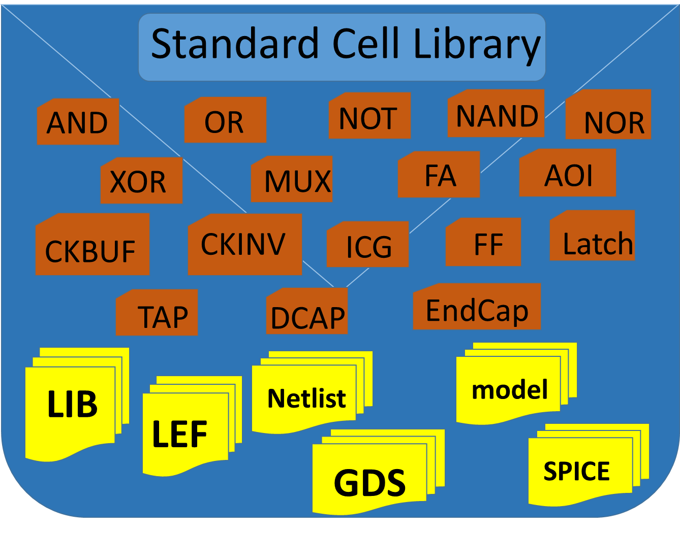
A standard cell library contains a rich variety of cells that serve different purposes in a design. They can be grouped into several categories.
This article provides a clear, concise breakdown of the typical cell types found in a modern library.
Read the introduction under "What Is a Standard-Cell Library?" and then focus on the table in the section "What’s Inside a Standard-Cell Library?". This table gives you an excellent overview of the different cell categories.
As you saw in the reading, the main categories are:
- Combinational Logic Cells: These are the stateless building blocks like
AND,OR,NAND,XOR. Libraries also include more complex cells likeAND-OR-Invert(AOI) because they can be more efficient in area and speed than building the same function from multiple simpler gates. - Sequential Logic Cells: These cells have memory. The most common is the D-type Flip-Flop (
DFF), which is the fundamental building block for registers, counters, and FSMs. Latches are also included but are used less frequently in modern synchronous design. - Specialty and Timing Cells: This includes a wide range of buffers and inverters, which don't perform logic but are crucial for driving long wires or fixing timing violations. Libraries provide these cells in multiple drive strengths (e.g., 1X, 2X, 4X). A higher drive strength cell is faster and can drive a larger load, but it also consumes more power and area.
- Physical Cells: These cells have no logical function but are essential for the physical integrity of the chip.
- Filler Cells: Fill in the empty spaces in a row of standard cells to ensure electrical continuity for the power rails.
- Tap Cells: Connect the silicon substrate to the power or ground network to prevent a destructive condition known as latch-up.
- Decoupling Capacitors (Decaps): Act as small, local charge reservoirs to stabilize the power supply voltage.
The image below provides a great visual summary of the variety of cells and the different output files they generate, which we will discuss next.
3. The "Views": Different Files for Different Tools
A standard cell library isn't a single file. It's a collection of data files, where each file provides a different "view" of the cells, optimized for a specific tool in the design flow. This is a powerful form of abstraction.
The three most important views for a designer are the timing (.lib), physical (.lef), and behavioral (.v) models.
File Formats in a Standard-Cell Library
This section of the VLSIFacts article explains the purpose of the most common file formats that make up a standard cell library.
Read the section "File Formats in a Standard-Cell Library" and pay close attention to the purpose of the .lib, .lef, .gds, and .v files.
To supplement this, let's explore these key files in a bit more detail using another resource.
Digital VLSI Design Lecture 4: Standard Cell Libraries
These slides offer a more technical look at the concept of abstraction and then dive into the details of the LEF and Liberty formats.
First, review the slide titled "My favorite word… ABSTRACTION!" and the following one, "What files are in a standard cell library?". This reinforces the idea of different views for different tools. Next, read the slides under the "Library Exchange Format (LEF)" heading. This explains the physical abstract view used for placement and routing. Finally, read the slides under "Liberty Timing Models (.lib): Introduction". This describes the timing view, which is critical for synthesis and timing analysis.
Now, let's hear from an expert who actually builds these libraries. James Stine is a professor who created some of the first open-source standard cell libraries. In this clip, he describes the tools and processes he uses.
Crafting open source standard cell libraries with James Stine
In this video from the Zero To ASIC Course, James Stine discusses his practical workflow for creating standard cell libraries.
Watch the segment from his discussion on tool flow. Listen for how he mentions: Magic: A tool for creating the physical layout (which becomes the .gds file). Characterization: The process of running simulations (SPICE) to generate performance data. Liberty file: The output of characterization, containing the timing and power information. Place and Route tools: The downstream tools that consume these library files. Track height: A key physical characteristic of a standard cell library.
4. Role in the Design Process
Let's tie this all together by tracing how these library views are used in the two main stages you're learning about: synthesis and physical design.
Role in Logic Synthesis
As you learned in the last lesson, the synthesis tool's job is to convert your RTL into a gate-level netlist. It relies almost exclusively on the Liberty (.lib) file.
- Translation: The tool parses your RTL, e.g.,
assign y = a & b;. - Mapping: It understands this is an AND function. It then consults the
.libfile to find all cells that perform this function (e.g.,AND2_X1,AND2_X2,AND2_X4, where 'X' denotes drive strength). - Optimization: Based on the timing constraints you provided (your SDC file), the tool chooses the best cell. If the path is slow, it might pick a high-drive-strength
AND2_X4. If the timing is easily met, it will pick a smaller, lower-powerAND2_X1to save area and power.
The output is a gate-level netlist that instantiates specific cells from the library, like AND2_X1 U1 (.A(a), .B(b), .Y(y));.
Role in Physical Design (Place & Route)
The physical design tools take the gate-level netlist from synthesis and create the actual chip layout. These tools primarily use the Library Exchange Format (.lef) file.
- Placement: The placement tool reads the netlist and sees it needs to place an
AND2_X1cell. It looks upAND2_X1in the.leffile to find its physical dimensions (height and width). It then places this rectangular block on the chip floor, typically in neat rows with other cells. It does this for all the millions of cells in the design. - Routing: After all cells are placed, the routing tool uses the
.leffile again. It looks at the pin information for each cell—the exact location of inputsA,B, and outputYon the cell's boundary—and connects them with metal wires according to the netlist. - Static Timing Analysis (STA): After routing, the timing analysis tools re-use the
.libfile. They combine the cell delays from the.libfile with the actual wire delays (calculated from the physical routes) to perform a final, highly accurate check to ensure the design meets its performance goals.
Conclusion
You now see that the standard cell library is far more than just a simple list of gates. It's a sophisticated and fundamental component of the ASIC design flow, providing different, highly-specialized models of each logic cell for each stage of the design process.
Key Takeaways:
- A standard cell library is a collection of pre-designed and characterized building blocks (cells) for a specific foundry process.
- It contains various views (data files) for different EDA tools. The main ones are:
- Liberty (
.lib): The timing/power view for synthesis and timing analysis. - LEF (
.lef): The physical abstract view for placement and routing. - GDSII (
.gds): The full layout view for manufacturing and final verification.
- Liberty (
- The synthesis tool uses the
.libfile to choose the optimal cells to meet performance, power, and area (PPA) targets. - The place and route tools use the
.leffile to physically arrange the cells and wire them together.
In our next lesson, we will focus on the details of those physical design steps, placement and routing, building directly on your understanding of how they use the LEF file to construct the chip layout.