Hello! In our last lesson, we saw how the abstract netlist is transformed into a physical chip layout through placement and routing. We ended with a crucial question: the chip is laid out, but how do we confirm it will run at the target speed?
Today's lesson answers that question. We will dive into one of the most critical signoff steps in the entire ASIC flow: Static Timing Analysis (STA). This is the process that verifies whether the millions of signals in your design will arrive at their destinations on time.
Your learning goal for this lesson is to explain the purpose of Static Timing Analysis (STA) in verifying timing constraints. You will learn what STA is, why it is preferred over other methods, what fundamental checks it performs, and how to interpret its results.
1. What is Static Timing Analysis?
After the physical design tools have placed and routed your design, they have created a layout with real, physical wires. These wires have resistance and capacitance, which introduce delays. STA is the process of calculating these delays to ensure no timing rules are violated.
Let's start with a video that introduces the concept and explains why it's so vital in modern chip design.
Introduction to Static Timing Analysis | STA , Physical Design, Synthesis in VLSI
This video, "Introduction to Static Timing Analysis," provides a high-level overview of why timing is a major concern and defines what STA is and what it does.
First, watch the introduction to understand why timing analysis is so critical for high-frequency designs. Next, watch the segment that defines STA and contrasts it with "dynamic" analysis (i.e., timing simulation). Pay close attention to why it's called "static." Finally, watch the part explaining the main purpose of STA, which is to validate that the design can operate at its rated speed.
As the video explained, STA is a "static" method because it analyzes the design without simulating any specific input data. Instead, it exhaustively checks every possible path in the design mathematically. This has two major advantages over running simulations with timing information (dynamic analysis):
- Completeness: It checks all paths, not just those exercised by a particular set of test inputs. This ensures you don't miss a critical timing violation that your simulation simply didn't trigger.
- Speed: It's significantly faster than running simulations, which is essential for today's billion-transistor chips where simulation would be impossibly slow.
To perform its analysis, an STA tool needs several key inputs, which we have encountered in previous lessons.
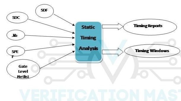
2. Verifying the Fundamental Timing Constraints
The core purpose of STA is to check every relevant path against the timing constraints you've defined. These constraints are primarily based on the setup and hold times of the flip-flops in your design—concepts you'll recall from our module on sequential logic.
- Setup Time (Max-Delay Check): This ensures data from a "launch" flip-flop arrives at a "capture" flip-flop before the next clock edge. This check determines the maximum clock frequency the chip can run at. It's a "max-delay" problem because we're worried the path is too slow.
- Hold Time (Min-Delay Check): This ensures that new data from a "launch" flip-flop doesn't arrive at the "capture" flip-flop too early, overwriting the data that is currently being captured. This is a "min-delay" problem because we're worried the path is too fast.
The following video explains the equations that form the basis of these two checks. Given your background in electrical engineering, you should find the mathematical formulation quite intuitive.
VLSI - Lecture 7e: Basic Timing Constraints
This video, "Basic Timing Constraints," provides a detailed walkthrough of the fundamental equations for setup and hold analysis.
Start by watching the introduction to the max-delay (setup) and min-delay (hold) problems. Next, focus on the detailed explanation of the max-delay (setup) constraint. Pay attention to the components that make up the data path delay: T_{CQ} (clock-to-Q delay of the launch flop), T_{logic} (delay of the combinational logic), and T_{setup} (setup time of the capture flop). Then, watch the explanation of the min-delay (hold) constraint. Note how this check is independent of the clock period. Finally, watch the summary which crystallizes the two main timing equations.
The Concept of Slack
The most important metric that STA tools calculate is slack. Slack is the difference between when a signal is required to arrive and when it actually arrives.
- Positive Slack (+): The timing constraint is met. The signal arrived earlier than required.
- Negative Slack (-): The timing constraint is violated. The signal arrived too late (for setup) or too early (for hold).
Let's solidify this with a simple example for a setup check.
Beginner's Static Timing Analysis Guide
This section of the guide provides a very clear, numerical example of how slack is calculated for a setup check.
Read the section titled "Real-World Example to Understand STA Easily." Follow the simple calculation for both the "PASS" and "FAIL" scenarios to see how slack directly tells you if timing is met.
3. STA in Practice: Reports and Corners
In a real ASIC flow, STA is not just a single check. It's performed at multiple stages and under various operating conditions, known as Process, Voltage, and Temperature (PVT) corners. This ensures the chip works whether it's running hot on a hot day with low voltage, or cold on a cold day with high voltage.
- Setup checks are typically performed at the slow corner (e.g., low voltage, high temperature, slow process silicon) because this represents the worst-case scenario for a path being too slow.
- Hold checks are performed at the fast corner (e.g., high voltage, low temperature, fast process silicon) because this is the worst-case for a signal arriving too quickly.
The output of an STA tool is a detailed report that shows the slack for the most critical paths. Let's look at how to interpret a basic STA report.
This article from the Zero to ASIC course shows excerpts from real STA reports generated by the open-source tool OpenSTA.
Read the section "Min report - validating hold timing." Look at the report and see how it traces a path from a startpoint to an endpoint. Find the "data arrival time," the "data required time," and the final "slack (MET)" value. Next, read "Max report - validating setup timing." Again, trace the path in the report. This time, notice that the slack is negative, resulting in a "slack (VIOLATED)" status. This is a real timing failure that would need to be fixed.
As these reports show, STA gives the designer a precise, actionable list of timing violations. Fixing these violations—a process called timing closure—involves various techniques, such as swapping slow cells for faster ones, inserting buffers, or re-routing critical wires. This iterative process continues until all paths have positive slack.
Conclusion
In this lesson, we explored the critical role of Static Timing Analysis in the ASIC design flow. You've learned that it's the gatekeeper that ensures a physically designed chip can meet its performance targets.
Key Takeaways:
- Purpose of STA: To verify that a digital circuit meets its timing requirements (rated speed) without running exhaustive, time-consuming simulations.
- Static vs. Dynamic: STA is "static" because it mathematically analyzes all paths without needing input stimuli, making it fast and complete.
- Core Checks: STA's fundamental task is to verify setup (max-delay) and hold (min-delay) constraints for all sequential elements in the design.
- Slack is Key: The result of a timing check is slack. Positive slack means the timing is met; negative slack indicates a violation that must be fixed.
- Practical Application: STA is run across various PVT corners to ensure robust operation, and its reports pinpoint the exact paths that are failing.
You now understand how we verify that the design is fast enough. However, being fast is not enough. The design must also be manufacturable. In our final lesson of this module, we will look at physical verification, which involves checks like DRC and LVS, to ensure the layout adheres to the foundry's manufacturing rules.