Welcome to the final lesson of your course! I hope you're proud of the progress you've made, starting from the fundamentals of number systems and now arriving at the last step before a chip design is sent for manufacturing.
In our last lesson, we focused on Static Timing Analysis (STA), the critical process that verifies your design is fast enough to run at its target clock speed. We learned how STA checks every path for setup and hold violations. But being fast isn't the only requirement. The design must also be physically manufacturable and electrically correct.
This lesson concludes our journey through the ASIC design flow by exploring physical verification. Your learning outcome is to describe the purpose of physical verification checks like DRC (Design Rule Check) and LVS (Layout vs. Schematic). These are the final "signoff" checks that give the green light to send your chip design to the fabrication plant, a process known as "tapeout."
1. Design Rule Check (DRC): The Manufacturing Rule Keeper
After place-and-route, you have a complete physical layout of your chip, typically in a file format called GDSII. But how do you know if the microscopic patterns in this layout can actually be created reliably in a silicon factory (a "fab")? This is where the Design Rule Check (DRC) comes in.
The foundry that will manufacture your chip provides a "rule deck," which is a set of geometric constraints your layout must obey. DRC is an automated process that checks your entire layout against these rules.
Think of it like a building code inspection for your chip. The architect's plans might be beautiful and structurally sound (like your RTL design), but a building inspector (the DRC tool) must verify that every wire, pipe, and support beam meets specific safety and construction standards (the foundry's rules).
To understand why these rules are so important, let's watch a short video.
This video, "Design Rule Check," explains what design rules are and why they are a necessary interface between the chip designer and the fabrication process engineer.
Watch the first segment, "What is a design rule?", which introduces the concept of DRC. Pay attention to the explanation of how these rules prevent manufacturing defects like short circuits or open circuits due to fabrication imperfections.
As the video explains, these rules are necessary because the chip fabrication process is not perfect. DRC ensures there is enough margin in the layout to tolerate small variations during manufacturing. A failure to meet these rules (a "DRC violation") could lead to a chip that doesn't work at all.
DRC violations fall into several categories, but they all relate to the geometry of the layout. The most common rules involve:
- Minimum Width: Ensures a wire is not too thin, which could cause it to break (an "open circuit").
- Minimum Spacing: Ensures two adjacent wires are not too close, which could cause them to touch (a "short circuit").
- Enclosure/Overlap: Ensures one layer correctly covers another, for example, that the metal layer fully encloses a via (a connection between layers).

If DRC finds a violation, the layout must be fixed and re-checked until the design is "DRC clean."
2. Layout Versus Schematic (LVS): The Electrical Matchmaker
A DRC-clean design is manufacturable, but is it the correct circuit? The place-and-route tool works with millions of components and connections. It's possible for a bug in the tool or a manual edit to create a layout that is physically valid (passes DRC) but does not match the intended logic from your Verilog code.
Layout Versus Schematic (LVS) is the check that ensures the physical layout is electrically identical to the original design plan. Here, the "schematic" refers to the gate-level netlist that was created by the synthesis tool.
The LVS process involves two key steps:
- Extraction: The LVS tool analyzes the geometric shapes in the layout (the GDSII file) to identify transistors, standard cells, and their interconnections. It "extracts" this information to create a new, layout-based netlist.
- Comparison: The tool then compares this extracted netlist against the original source netlist.
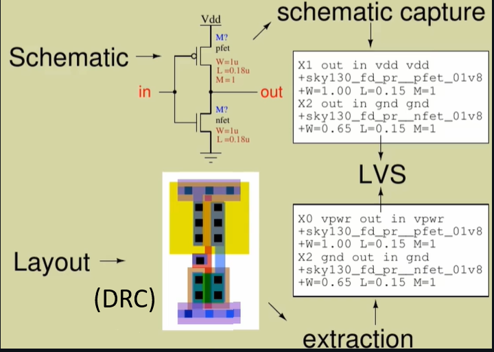
The LVS tool checks for:
- The total number of devices (e.g., standard cells).
- The types of devices.
- The number of nets (wires).
- The connectivity between all devices.
If everything matches, the design is "LVS clean." If not, the tool reports errors like:
- Shorts: Two nets that should be separate are connected in the layout.
- Opens: A net that should be continuous is broken in the layout.
- Component Mismatches: The layout contains a different number or type of components than the schematic.
The following video explains how LVS works in a modern digital design flow.
Digital-on-top Physical Verification (Fullchip LVS/DRC) - Part 1
This video, "Digital-on-top Physical Verification," explains the concept and flow of LVS, particularly in the context of a digital design created with place-and-route tools.
First, watch the segment that explains what LVS is. It emphasizes that LVS compares the layout to the intended design. Next, watch the overview of the LVS flow. This part details how the source netlist and layout netlist are generated and then compared. Notice the "extraction" step which is key to creating the netlist from the layout.
3. Putting It All Together: DRC and LVS
It's crucial to understand that DRC and LVS are independent checks that verify two different things. A design must pass both to be considered ready for fabrication.
- DRC checks the physics: Is the layout manufacturable according to the foundry's rules? It only looks at the layout geometry.
- LVS checks the logic: Does the manufactured layout implement the correct circuit function? It compares the layout against the source netlist.
To solidify this distinction, the following short article provides a perfect summary.
DRC vs LVS: Design Rule Checking and Layout Verification Explained
This post by Ezekiel Adeosun provides a concise and clear explanation of the difference between DRC and LVS.
Read the short sections titled "DRC: The Manufacturing Rule Keeper" and "LVS: The Electrical Matchmaker." Pay close attention to the simple analogies used for each and the final summary of how they work together as a team.
A design can be DRC clean but fail LVS (e.g., a wire is connected to the wrong input, but all spacing rules are met). Conversely, a design could be LVS clean but fail DRC (e.g., two wires are too close together, but all connections are logically correct). A successful tapeout requires both checks to pass without any errors.
Conclusion
Congratulations on completing the final lesson! You have now journeyed through the entire ASIC design flow, from writing RTL code to performing the final signoff checks that ensure a design is correct, meets timing, and is ready for fabrication.
Key Takeaways:
- Physical verification is the final step before tapeout, ensuring the physical layout is correct and manufacturable.
- Design Rule Check (DRC) acts as a "building code inspector," verifying that the layout's geometry adheres to the foundry's manufacturing rules to prevent defects like shorts and opens.
- Layout Versus Schematic (LVS) acts as an "electrical matchmaker," verifying that the extracted circuit from the layout is functionally identical to the source netlist from synthesis.
- A design must be both DRC and LVS clean to be taped out.
You began this course with the goal of preparing for your Open Silicon Bootcamp, and you've built a strong foundation covering digital logic, Verilog, and the complete ASIC flow. You should feel confident in your understanding of how a digital idea becomes a physical reality.
Best of luck with your bootcamp and your future in the exciting world of chip design