Hello! In our last lesson, we established that modern digital circuits are synchronous, meaning their state changes are orchestrated by the edges of a clock signal. This approach brings order and predictability, preventing the race conditions that can plague level-triggered designs.
Now, we'll introduce the fundamental building block that makes this all possible: the D-type flip-flop. This is the most important memory element in digital design. Your goal for this lesson is to be able to describe its behavior completely using its circuit symbol, its characteristic table, and, most importantly, its timing diagram.
1. The D-Type Flip-Flop: A Controlled Memory Cell
A flip-flop is a circuit that can store a single bit of information (a 1 or a 0). The "D" in D-type flip-flop stands for "Data." Its job is incredibly simple but powerful: on the active edge of the clock, it looks at its D input and stores that value. At all other times, it ignores the D input and holds its stored value steady.
Let's start with a foundational reading that introduces the D flip-flop and its standard symbol.
Circuit and Operation of a D Flip-Flop
Read the first part of this article from All About Circuits.
Focus on the introduction up to and including Figure 2. Pay attention to: The distinction between a level-triggered latch and an edge-triggered flip-flop. The terminals of the flip-flop: D, C (Clock), Q, and Q̅. The simple truth table (Table 1) and the timing diagram (Figure 2), which give a first look at the flip-flop's behavior.
As the article mentions, the D flip-flop is the workhorse of digital memory. A key concept that distinguishes it from the level-triggered latches we discussed previously is that it samples the input at an instant, rather than following it over a duration.
The following short video segment explains this "sample versus follow" idea very clearly.
Watch this brief introduction from the "D Flip Flops" video by Columbia Gorge Community College.
Focus on the explanation from D Latch to D Flip-Flop. The key takeaway is that an edge-detection circuit is added to a latch to create a flip-flop, changing its behavior from "following" the D input to "sampling" it on the clock edge.
2. Characteristic Table and Equation
To formally describe the behavior of a flip-flop, we use a characteristic table. This table defines the flip-flop's next state, which we denote as , based on its current input(s) and sometimes its current state, .
Let's look at the characteristic table for the D flip-flop.
Review the section "Characteristic Table of D Flip Flop" in this article.
Examine the table. It shows the next state, Qn+1, for every combination of the input D and the current state, Qn.
Notice something interesting in that table? The next state depends only on the D input. The current state is irrelevant! This makes the D flip-flop's behavior very straightforward.
This relationship can be captured in a simple algebraic expression called the characteristic equation. For the D flip-flop, it is the simplest one possible:
This equation states that "the next state of the output Q will be whatever the D input is at the active clock edge."
3. Timing Diagrams: Visualizing Behavior Over Time
The most practical way to understand and debug sequential circuits is through timing diagrams. These diagrams show how the signals in a circuit change over time. Let's analyze the behavior of a positive-edge-triggered D flip-flop, which acts on the rising (0-to-1) edge of the clock.
The following video provides an excellent, step-by-step walkthrough. The key is to first identify the active clock edges and then see what the D input is doing at those exact moments.
Continue with the "D Flip Flops" video to see timing analysis in action.
First, watch the walkthrough of the first example. Notice how the instructor marks all the positive clock edges before determining the output Q. Next, watch the second example. This part highlights a common point of confusion: the flip-flop triggers on the edge of the clock, not on any changes in the D signal. Q only changes after a clock edge, even if D changes many times between edges.
Flip-flops can also be negative-edge-triggered, acting on the falling (1-to-0) edge of the clock. The circuit symbol for a negative-edge-triggered device includes a small bubble at the clock input. The behavior is identical, just shifted to the falling edge.
This next video segment provides a great side-by-side comparison for the same input signals, making the difference between positive and negative edge-triggering very clear.
D Flip-Flop Explained | Truth Table and Excitation Table of D Flip-Flop
Watch this segment from "D Flip-Flop Explained" by ALL ABOUT ELECTRONICS.
Observe the timing diagrams for both positive and negative edge triggering. Note that the shape of the Q output waveform is the same in both cases, but its transitions are aligned with either the rising or falling edges of the clock.
Summary of D Flip-Flop Behavior
We've now seen the D flip-flop described in three ways: with its symbol, its characteristic table/equation, and its timing diagram. The image below brings these three representations together perfectly.
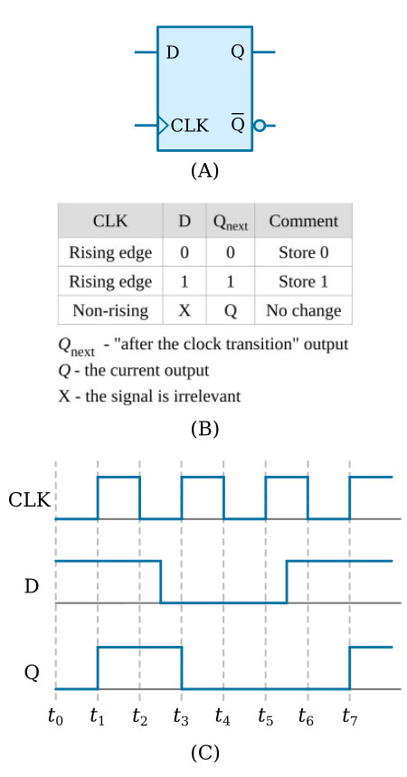
This single image encapsulates everything you need to know about the basic operation of a D flip-flop.
Conclusion
In this lesson, you've been introduced to the D-type flip-flop, the fundamental memory element of synchronous digital logic. We have defined its behavior precisely and seen it in action.
Here are the key takeaways:
- A D-type flip-flop is an edge-triggered memory device that stores one bit.
- Its core function is to sample the
D(data) input on the active clock edge and transfer that value to theQoutput. - At all times other than the active clock edge, the
Qoutput holds its previous value, ignoring changes at theDinput. - The characteristic equation, , mathematically describes this behavior.
- Timing diagrams are essential tools for visualizing how the
Qoutput responds to theDand clock inputs over time.
So far, we've assumed our flip-flop works perfectly. In the real world, however, there are physical limitations. For the flip-flop to reliably capture the data, the D input must be stable for a small window of time around the clock edge. In the next lesson, we will explore these critical timing parameters, known as setup and hold time.