Hello! In our last lesson, we explored the D-type flip-flop as an ideal component that perfectly samples data on a clock edge. This gave us a powerful tool for building synchronous circuits.
Today, we move from the ideal to the real world. Flip-flops are physical devices built from transistors, and they have timing limitations. For a flip-flop to reliably capture data, the data signal must be stable for a small window of time around the active clock edge. This lesson will explain these critical timing requirements, known as setup and hold time. Mastering these concepts is fundamental to designing any reliable, high-speed digital circuit, which is a core skill for the ASIC design flow you're preparing for.
1. Defining the Timing Window: Setup and Hold
In a synchronous system, all data transfers are orchestrated by the clock. For a successful transfer between a source flip-flop and a destination flip-flop, the data arriving at the destination flip-flop's D input must respect two rules relative to its clock edge.
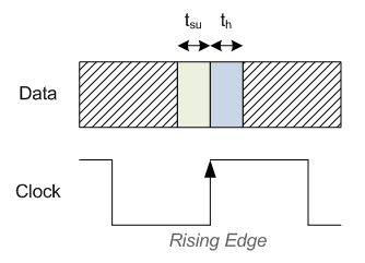
- Setup Time (): The minimum amount of time the data input must be stable before the active clock edge arrives.
- Hold Time (): The minimum amount of time the data input must remain stable after the active clock edge has passed.
Together, these two times create a "keep-out" window around the clock edge where the data input must not change.
The following short video provides a very clear and concise definition of these two essential concepts.
Setup, Hold, Propagation Delay, Timing Errors, Metastability in FPGA
Watch this brief segment from the "Setup, Hold, Propagation Delay" video by nandland.
Focus on the straightforward definitions provided for setup and hold time. The key idea is "setup before the clock, hold after the clock."
This timing diagram provides a perfect visual summary of these definitions.
2. Why Do These Times Exist? A Look Inside the Flip-Flop
Setup and hold times are not arbitrary rules; they are direct consequences of the physical construction of a flip-flop. Since you have a background in electrical engineering, you'll appreciate that signals take a finite amount of time to propagate through transistors and wires.
As we saw briefly in the previous lessons, a D flip-flop is typically built from two latches (master and slave) connected in series. Let's look at how this internal structure dictates the need for setup and hold times.
The following video explains the physical origins of these requirements by looking at the behavior of the internal transmission gates and inverters.
Digital Design Interview Questions | Setup and Hold Time in Flip-Flop and Latch | Static Timing
Watch these two segments from "Digital Design Interview Questions" by Flop_n_Adder to understand the physical basis for setup and hold time.
First, watch the explanation of why setup time is required. It shows how the data needs time to travel through the master latch's internal components and stabilize before the clock edge effectively "closes the door." Next, watch the segment on why hold time is required. This explains that the "door" (the input transmission gate) doesn't close instantly. The hold time ensures the input data remains stable long enough to prevent the next data value from corrupting the value that is currently being latched.
In summary:
- Setup time exists to ensure the data signal has enough time to propagate through the master latch's logic and settle to a stable value before the master latch is disabled by the clock edge.
- Hold time exists to protect the just-latched data from being corrupted by changes at the
Dinput that might "leak through" while the input transmission gate is in the process of closing.
3. Consequences of Violations: Metastability
If the data at the D input changes during the setup or hold window, we have a timing violation. This violation can put the flip-flop into a dangerous state called metastability.
A metastable state is an unstable, intermediate state where the output is not a valid '0' or '1'. It might oscillate or hover at a voltage halfway between high and low. Eventually, the flip-flop will randomly settle to either a '0' or a '1', but the time it takes to do so is unpredictable. In a synchronous system, such unpredictable behavior is a critical failure.

4. Setup and Hold in a Timing Path
Let's now analyze these concepts in the context of a typical digital circuit path: a launch flip-flop (FF1) sends data through some combinational logic to a capture flip-flop (FF2).
This diagram from the JLCPCB blog post shows a standard timing path between a launch flop and a capture flop, with combinational logic in between. This is the fundamental structure for timing analysis.
Several delays are involved here:
- Clock-to-Q Delay (): The time it takes for data to appear on the Q output of FF1 after a clock edge.
- Logic Delay (): The propagation delay through the combinational logic cloud.
- Clock Skew (): The difference in arrival time of the clock signal at FF1 and FF2.
Setup Time Analysis
For the circuit to work correctly, the data from FF1 must arrive at FF2's D input before FF2's setup time window begins. The total time it takes for data to travel from FF1 to FF2 is . This entire path must be shorter than one clock period, with enough time left over for the setup time of FF2.
The condition to avoid a setup violation is:
Here, is the longest possible (worst-case) delay through the logic. Setup violations happen when the logic path is too slow or the clock frequency is too high. This is why setup analysis determines the maximum operating frequency of your design.
Hold Time Analysis
A hold violation occurs if the data from a new clock cycle arrives at FF2 too soon, changing before FF2 has had a chance to securely hold the data from the previous cycle.
The condition to avoid a hold violation is:
Here, is the shortest possible (best-case) delay through the logic. Hold violations happen when the logic path is too fast. Notice that the clock period () is not in this equation. Hold violations are independent of the clock frequency.
To see how these checks are performed in practice, let's look at an article that presents these concepts with a numerical example.
Understanding Digital Circuit Timing
Please read the following sections from the JLCPCB blog post to see the formal equations and a practical example.
Start by reading the definitions under the headings "Setup Time" and "Hold Time". Next, review the equations under "Timing Equations". Don't worry about memorizing them, but understand what each term represents. Finally, walk through the "Worked Numerical Example". Pay close attention to how they calculate the slack (the margin by which timing is met or missed) and notice how a path can pass the setup check but fail the hold check.
Conclusion
In this lesson, we've moved beyond the ideal flip-flop to understand its real-world physical constraints. These timing requirements are not just theoretical—they are the foundation of Static Timing Analysis (STA), a critical step in the ASIC design flow where automated tools check every single path in a design for these violations.
Here are the key takeaways:
- Setup time () is the window before the clock edge where data must be stable. Violations occur on slow paths and limit the maximum clock frequency.
- Hold time () is the window after the clock edge where data must remain stable. Violations occur on fast paths and are independent of clock frequency.
- Violating these times can cause metastability, an unpredictable state that is fatal to a synchronous design's reliability.
- Timing analysis involves considering the delays in a full path: clock-to-q delay, logic delay, and setup/hold times.
Now that you understand how a single bit is stored reliably in a D flip-flop, we are ready to build larger structures. In the next lesson, we will combine multiple flip-flops to create a 4-bit register, a circuit capable of storing a multi-bit data value.