Hello! In our previous lesson, we drew a clear line between combinational circuits, which are stateless, and sequential circuits, which use memory to influence their outputs. You learned that sequential circuits need a way to control when their memory is updated, and we briefly mentioned the role of a clock signal.
Today, we're going to zoom in on that concept. This lesson is all about the "heartbeat" of digital systems. We will explore the role of the clock signal in detail and understand a critical concept for modern digital design: edge-triggered behavior. This is a foundational topic for building any kind of memory-based circuit, from a simple counter to a complex processor.
1. Synchronous Systems and the Clock Signal
In the last lesson, we saw that sequential circuits use feedback to store a state. If the inputs to the logic block change, the state could change, which then feeds back and could cause another change. To prevent this chaotic chain reaction, we need to bring order to the system. This is done by making the circuit synchronous.
In a synchronous system, all state changes across the entire circuit happen at the exact same time, orchestrated by a shared timing reference: the clock signal.
The following video introduces the idea of synchronous circuits and then describes the characteristics of the clock signal that drives them.
Introduction to Sequential Circuits | Digital Electronics
Watch this segment from the video "Introduction to Sequential Circuits" by ALL ABOUT ELECTRONICS.
First, watch the part that distinguishes between synchronous and asynchronous circuits. Almost all modern digital design, and everything we will do, is synchronous. Next, focus on the introduction to the clock signal itself. Pay attention to the terminology: period, ON time, OFF time, duty cycle, and the concepts of rising and falling edges.
To summarize, a clock is a periodic signal that oscillates between a low voltage (logic 0) and a high voltage (logic 1). Its purpose is to provide a regular "tick" that tells all the memory elements in the circuit when to update their state. The two most important moments in a clock cycle are its transitions:
- Rising Edge (or Positive Edge): The transition from 0 to 1.
- Falling Edge (or Negative Edge): The transition from 1 to 0.
2. Triggering: Reacting to the Clock
A memory element in a synchronous circuit doesn't pay attention to its inputs all the time. It only "listens" when the clock tells it to. The specific way a circuit responds to the clock is called its triggering method. There are two main types: level-triggering and edge-triggering.
The next segment of the video you just watched explains this distinction clearly.
Introduction to Sequential Circuits | Digital Electronics
Continue watching the video from ALL ABOUT ELECTRONICS.
Watch the section that explains the difference between level-triggered and edge-triggered behavior. Note how a level-triggered circuit is sensitive for an entire duration (e.g., while the clock is high), whereas an edge-triggered circuit is only sensitive for an instant.
The image below provides a great visual summary of these concepts.

In modern digital design, and particularly for ASIC and FPGA development, edge-triggering is the standard. Almost everything is triggered on a single clock edge, most commonly the positive (rising) edge.
3. Why Edge-Triggering is Essential
This naturally leads to a crucial question: why is edge-triggering so strongly preferred over level-triggering? The reason is fundamental to creating stable, predictable, and reliable sequential circuits.
Level-triggering introduces a major risk known as a race condition. Because the memory element is "transparent" for the entire duration the clock is high, a change in its output can feed back through the combinational logic and arrive at its input within the same clock cycle, causing another change, and then another. This can lead to unpredictable oscillations or an incorrect final state.
Edge-triggering solves this problem elegantly. The "window" when the memory element is sensitive to its inputs is practically instantaneous (the moment of the clock edge). The input is sampled, the state is updated, and the element then becomes "opaque" again until the next active edge. This clean separation ensures that the output from one clock cycle's state change is only used to calculate the state for the next clock cycle.
The following discussion from a forum of engineers gives some excellent, practical insights into this topic.
Why edge triggering is preferred over level triggering?
Read the selected answers on this Stack Exchange page to get a deeper, practical understanding.
First, read the answer by the user "Kaz" starting with "The issue with level triggering is that while the clock level is high...". This clearly explains the feedback problem and why simply slowing down the clock makes it worse for level-triggered circuits. Next, read the short but powerful answer by "ajs410". The example of an 8-bit adder and a register provides a perfect illustration of the non-deterministic behavior of level-triggering versus the deterministic, predictable behavior of edge-triggering. Finally, read the answer by "quantum231". This answer connects edge-triggering to the concept of timing analysis, a critical step in the ASIC design flow that we will discuss later in the course. It highlights how edge-triggering makes timing verification manageable.
4. A Preview of Verilog for Edge-Triggering
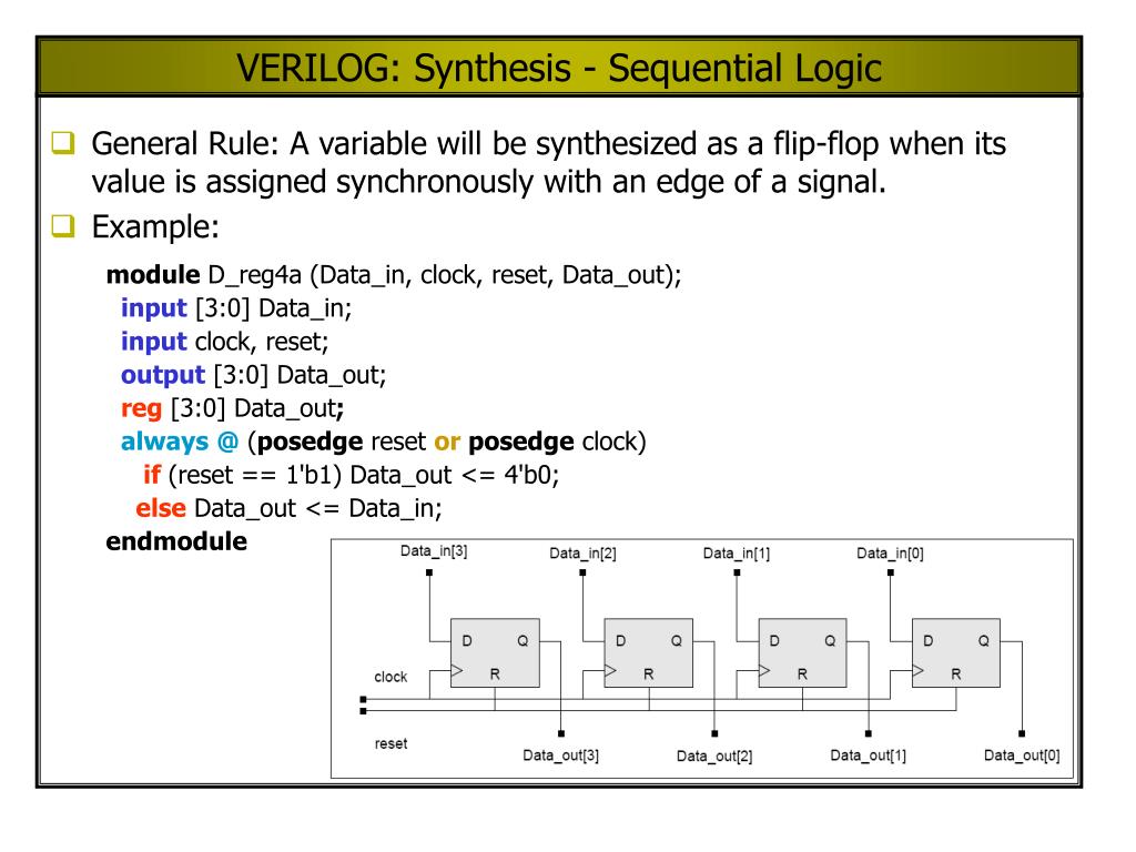
As you move into writing Verilog, you'll see this concept appear directly in the code. We tell the synthesis tools to create an edge-triggered circuit using a specific syntax within an always block.
For example, to make a process that happens only on the rising edge of a signal named clk, you would write:
always @(posedge clk)
The posedge keyword explicitly tells the tool to create logic that is sensitive only to the low-to-high transition of the clk signal. This is the standard way to describe synchronous, sequential logic.
The image below shows how this Verilog code translates directly into hardware. The always @(posedge clk) construct is synthesized into a set of edge-triggered D-type flip-flops—the fundamental memory element we will study in the next lesson.
Conclusion
In this lesson, we've established the rhythm of synchronous digital systems. You now understand how a clock signal provides the timing, and more importantly, why the concept of edge-triggering is so critical for building reliable circuits.
Here are the key takeaways:
- Clock Signal: A periodic signal that synchronizes state changes in a digital system, ensuring orderly operation.
- Synchronous Design: A methodology where all memory elements share a common clock. This is the standard for modern digital logic.
- Level-Triggering: A memory element is active for the entire duration a clock signal is at a specific level (e.g., high). This is prone to race conditions and is generally avoided.
- Edge-Triggering: A memory element updates its state only at the precise instant of a clock transition (rising or falling edge). This prevents race conditions and leads to predictable, analyzable circuits.
- Verilog: We use keywords like
posedgeto explicitly define edge-triggered behavior in our hardware description.
We've covered the when of state changes. In our next lesson, we will look at the what—the fundamental building block that actually stores the data at that clock edge: the D-type flip-flop. You will learn its structure, how it behaves, and see its characteristic table.