Hello! In our last lesson, we established the fundamental difference between a Hardware Description Language (HDL) and a software programming language. You learned that HDLs like Verilog are used to describe a concurrent hardware circuit, not to write a sequence of instructions.
Today, we move from concept to practice. You will learn how to write the basic structure of any Verilog design: the module. A module is the fundamental building block in Verilog, much like a schematic for a single component. Our goal is to define a module's interface—its inputs and outputs—and the internal signals it uses. This is the first step in translating the logic diagrams we've studied into a format that design tools can understand.
1. The Anatomy of a Verilog Module
Every piece of hardware you design in Verilog will be encapsulated within a module. Think of it as a black box with a specific function. You define what goes in, what comes out, and what happens inside.
Let's start with a video that walks through the basic syntax and structure of a Verilog module.
Verilog Basics - STRUCTURE of a Verilog Module | Starting out in Hardware Description Language (HDL)
This video from Visual Electric provides a clear and concise breakdown of a Verilog module's structure.
Watch the following sections of the video: First, watch the introduction explaining what a module represents in hardware. Next, focus on the section covering the module declaration, including the module keyword, the module name, and the list of ports (inputs/outputs). Then, pay attention to the part explaining how to declare port directions and internal signals. Finally, watch the summary on the consistent structure of all modules.
As the video explained, all Verilog modules follow a standard template. Using the modern Verilog-2001 standard, which you should use for all your designs, the structure looks like this:
module <module_name> (
  // Port declarations go here (inputs and outputs)
  <direction> <type> [width-1:0] <port_name>,
  ...
);

  // Internal signal declarations go here

  // Logic implementation goes here (we'll cover this later)

endmodule
Let's break down each part.
2. Defining the Interface: Ports
Ports are the "pins" of your module. They define how it connects to the outside world.
- Direction: Can be
input,output, orinout(for bidirectional signals). - Type: The data type of the signal. For now, we'll focus on
wireandreg. If you don't specify a type for a port, it defaults towire. - Width: Signals can be single-bit (a scalar) or multi-bit (a vector). A 4-bit bus would be declared with a width like
[3:0]. This notation[MSB:LSB]defines a vector from the most-significant bit to the least-significant bit.[3:0]is a 4-bit vector with bits indexed 3, 2, 1, and 0.
Let's look at a simple example. The image below shows the Verilog code for a 2-to-1 multiplexer alongside its circuit diagram. This should help you visualize how the code describes the hardware.
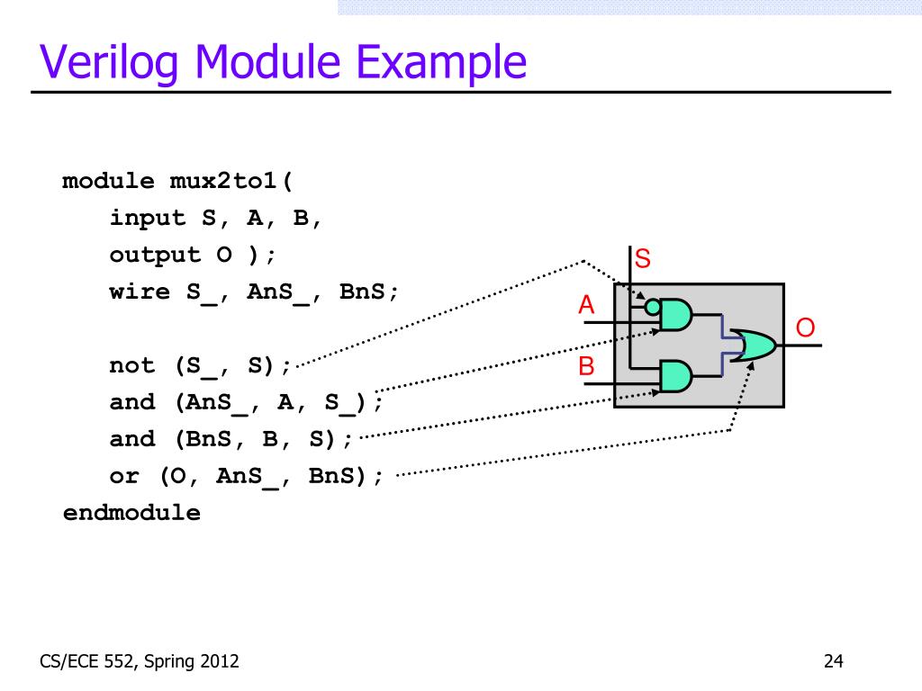
In this example, S, A, and B are single-bit inputs, and O is a single-bit output.
3. Declaring Signals: wire vs. reg
This is one of the most important and often confusing topics for beginners. In Verilog, the two primary data types you will use for synthesizable hardware are wire and reg.
- A
wireis like a physical wire. It's a connection between two points. It doesn't store any value itself; it simply passes a value from a driver to a destination. Wires are used to model combinational logic connections. - A
reg(for "register") is a variable that can store a value. It holds its value until a new value is assigned to it. Despite its name, aregdoes not always create a hardware register (like a flip-flop). It's simply a data type that has the ability to store data. We useregwhen describing both sequential logic (flip-flops) and combinational logic inside certain Verilog constructs.
The following video from Cadence, a major EDA (Electronic Design Automation) company, provides an excellent explanation of this distinction.
What Are the Differences Between Wire and Reg?
This video clearly explains the fundamental differences between the wire and reg data types.
Watch the entire video to understand: The core distinction between a wire as a connection and a reg as a storage element. How a reg retains its value. How a wire's value is determined by its drivers. Where they are declared and their default initial values in simulation (z for wire, x for reg).
To reinforce these concepts and highlight a common pitfall, let's turn to a textual resource.
This article from ChipVerify gives a detailed look at data types and provides excellent advice on avoiding common mistakes.
First, read the section "Nets and Variables" to see another explanation of wire and reg. Next, carefully read the section "Common Beginner Mistakes", focusing on Mistake #1: Confusing reg with Hardware Registers. This is a critical point that will save you a lot of confusion later.
Here is a summary of the key differences:
| Aspect | wire (Net) |
reg (Variable) |
|---|---|---|
| Hardware Model | A physical connection | A data storage element |
| Value Retention | No storage; must be continuously driven | Holds value until the next assignment |
| Typical Use Case | Connecting modules, output of assign statements |
Storing state in sequential logic (always @(posedge clk)), describing logic in combinational always blocks |
| Default Value | z (high-impedance) |
x (unknown) |
4. Internal Signals and Port Connection Rules
Just like a real circuit board has wires that only connect components on that board, a Verilog module often needs internal signals. These are signals that are not inputs or outputs. We declare them inside the module body, before the main logic.
Looking back at the MUX example, the signals S_, AnS_, and BnS_ are declared as internal wires used to connect the logic gates.
When connecting modules, there are strict rules about which data types can connect to which ports. The following diagram and rules are essential to remember.

Here's a summary of the rules for synthesizable code:
- An
inputport must be awireinside the module. It can be driven by either awireor aregfrom an external module. - An
outputport can be declared as awireor areginside the module. However, it must always connect to awirein the external module.
5. Your First Module Declaration
Let's put this all together with a practical exercise. Your task is to write the module declaration for a 4-bit register with a synchronous load enable.
Specifications:
- Module Name:
my_register - Inputs:
clk: 1-bit clock signalrst: 1-bit reset signalen: 1-bit load enable signald: 4-bit data input
- Output:
q: 4-bit data output
Think it through:
- Which signals are inputs and which are outputs?
- Which signals are vectors (multi-bit)?
- What should the data type of the output
qbe? Since a register's purpose is to store a value, its output should be declared as areg.
Here is the complete module declaration:
module my_register (
  input  wire        clk,
  input  wire        rst,
  input  wire        en,
  input  wire  [3:0] d,
  output reg   [3:0] q
);

  // The logic that describes *how* q is updated based on the inputs
  // would be written here. We will cover that in a future lesson on
  // sequential logic modeling.

endmodule
This code doesn't describe what the register does yet, but it perfectly defines its interface and the types of signals it uses. This is the first and most fundamental step in RTL design.
Conclusion
In this lesson, you've taken your first concrete step into writing Verilog. You've learned how to define the basic container for all hardware designs, the module, and how to declare its interface and internal signals.
Here are the key takeaways:
- A Verilog design is built from modules, which are defined between the
moduleandendmodulekeywords. - A module's interface is defined by its ports (
input,output), which have a direction, type, and width. - The two main synthesizable data types are
wire(for connections) andreg(for data storage). - It is critical to remember that
regis just a data type and does not always synthesize to a hardware register. - Modules can also have internal signals (wires or regs) that are not part of the external interface.
You now know how to create the "schematic" for a single hardware block. In our next lesson, we will build on this by learning how to connect these blocks together by instantiating one module within another.