Hello! In our last lesson, we examined the performance trade-off between throughput and latency that comes with pipelining. We established that while pipelining is essential for building high-speed processors, it's just one piece of the puzzle.
Today, we'll zoom out and look at the bigger picture. We will assemble all the individual digital building blocks we've discussed—like adders, multiplexers, and registers—into the fundamental structure of a simple processor. This lesson will introduce you to the processor datapath, which is the hardware that actually performs computations and moves data around. Understanding this architecture is a cornerstone of CPU design and will be essential knowledge for your upcoming bootcamp.
1. The Processor's Core: Datapath and Control
At a high level, a processor is divided into two main parts:
- Datapath: The "muscles" of the processor. It contains all the hardware units that perform operations on data, such as the arithmetic logic unit (ALU), registers for data storage, and the buses that connect everything.
- Control Unit: The "brain" of the processor. It decodes instructions from a program and generates control signals that command the datapath, telling it what to do, which data to use, and where to store the results.
Think of the datapath as a sophisticated workshop with various tools (ALU, memory) and workbenches (registers), and the control unit as the foreman directing the workflow according to a set of blueprints (the program instructions).
The following article provides a concise overview of the key functional units that make up a datapath.
Instruction Set Architecture — RISC-V — Single Cycle Datapath
This article introduces the main hardware blocks used in a simple RISC-V processor.
Start by reading the section "Functional Units Used" to get a quick summary of the four key components: the ALU, Register File, Memory Unit, and Control Unit. Also, review the section "Instruction Set Architecture: (ISA)" to understand the concept of programmer-accessible registers and the Program Counter.
Now, let's explore these components in more detail, following the logical flow of how a processor executes an instruction.
2. The Key Datapath Components
A processor executes instructions by moving data through a series of steps, often summarized as Fetch, Decode, Execute, Memory, and Write-back. Each step uses specific datapath components. The video below provides a great step-by-step construction of a simple datapath, which we will follow.
This video from "Down to the Wires" builds a single-cycle RISC-V datapath piece by piece, explaining the role of each component as it's added.
We will watch this video in segments as we discuss each component. For now, you don't need to watch anything, but keep it ready.
A. Instruction Fetch: The Program Counter (PC)
The very first step is to fetch the instruction the processor needs to execute.
- Program Counter (PC): This is a special-purpose register whose only job is to hold the memory address of the next instruction.
- Instruction Memory: This is a memory block that stores the machine code of your program. The PC provides the address, and the instruction memory outputs the corresponding instruction.
After an instruction is fetched, the PC must be updated to point to the next one. In a 32-bit architecture like RISC-V, instructions are 4 bytes long, so the PC is typically incremented by 4.
Watch this first part of the video to see these fetch components in action.
Watch the section on instruction fetch. Note how the Program Counter provides the address to the instruction cache (memory) and is then fed into an adder to calculate PC+4.
B. Execution: Register File and ALU
Once an instruction is fetched, the processor needs to perform the specified operation. This is the "Execute" stage.
- Register File: This is a small, extremely fast bank of registers located inside the processor. It acts as the processor's short-term "scratchpad" memory, holding the operands and results of ongoing calculations. Instructions specify registers to read from (e.g., source registers
rs1,rs2) and a register to write the result to (destination registerrd).
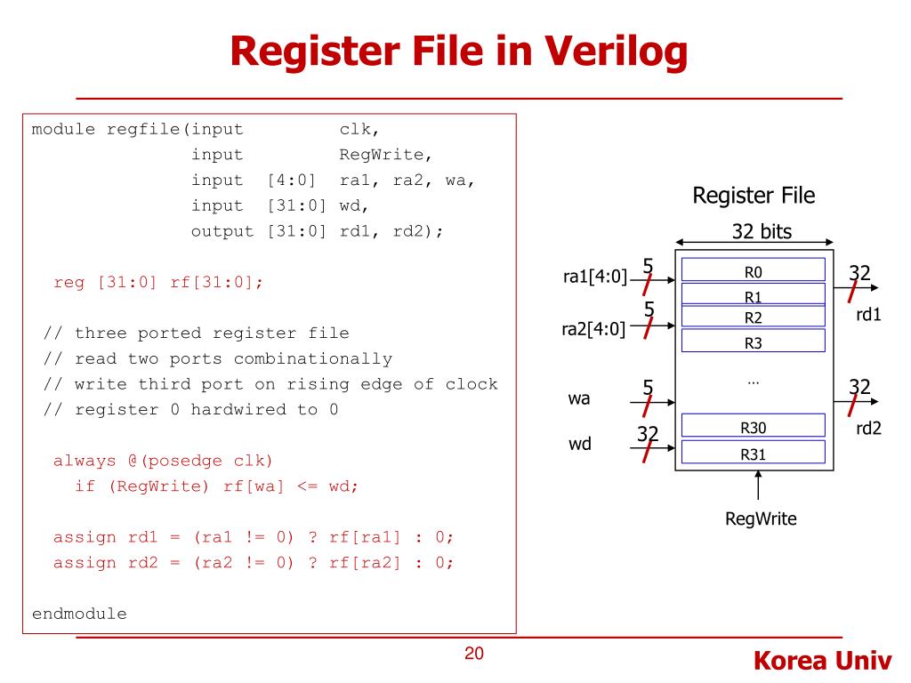
- Arithmetic Logic Unit (ALU): This is the computational heart of the datapath. It takes two operands as input (usually from the register file) and performs an operation like addition, subtraction, or a bitwise logical operation (AND, OR, etc.). A control signal from the Control Unit tells the ALU which specific operation to perform.
This lab manual introduces the ALU as the 'heart of a processor' and specifies its functions.
Read the "Introduction" to appreciate the ALU's central role. Then, review Table 1, "Summary of the ALU control" in Part 1. This table shows how a control signal (AluOp) selects different arithmetic and logical operations, which is a perfect example of how the control unit directs the datapath.
Now, let's see how the register file and ALU are connected to process data.
Watch the segment covering data processing. It shows how rs1 and rs2 from the instruction are used to read values from the register file, which are then fed into the ALU. The ALU result is then routed back to be written into the destination register rd.
Some instructions, known as I-type (immediate) instructions, use a small constant value embedded within the instruction itself as one of the operands. A multiplexer is used to select whether the ALU's second input comes from the register file or from this immediate value. You can see this being added in the video from
C. Memory Access: Loads and Stores
Not all data resides in the fast internal register file. load and store instructions are used to move data between the registers and the main data memory (which you can think of as the system's RAM).
- Data Memory: This component has inputs for an address, data to be written, and a write enable signal. It also has an output for data that is read.
- For a
loadinstruction, the ALU calculates a memory address, the processor reads from that address in Data Memory, and the retrieved data is written back to a register. - For a
storeinstruction, the ALU calculates a memory address, and data from a register is written to that address in Data Memory.
This next clip shows the integration of the data memory unit.
Watch the clip on loads and stores. Notice how the ALU is used to calculate the memory address and how a new multiplexer is added to choose whether the data written back to the register file comes from the ALU or from the data memory.
D. Control Flow: Branches and Jumps
Finally, programs are not always linear. Branches and jumps alter the flow of execution by changing the Program Counter to a new, non-sequential address. The datapath includes hardware to calculate these new "target" addresses and update the PC accordingly.
You can see this final piece being added from
3. Putting It All Together: Tracing an add Instruction
We've now seen all the major components. The image below shows a complete datapath for a simple MIPS processor, which is very similar to the RISC-V one we've been discussing.

Let's solidify this by tracing a simple R-type instruction, add rd, rs1, rs2, through the datapath. The following video provides an excellent animated walkthrough.
Instruction Breakdown/Datapath Tutorial
This video visually traces different instruction types through a MIPS datapath.
Watch the walkthrough of the R-type 'add' instruction. Follow the data from the register file to the ALU and back. Pay attention to how the control signals (shown as blue lines) configure the datapath for this specific operation: they enable register writing, select the ALU result to be written back, and ensure the PC simply increments by 4.
This trace perfectly illustrates how the datapath hardware is configured by control signals to execute a single instruction. Every instruction you write, whether in a high-level language like Python or C, is eventually compiled down to simple operations like this that are executed directly by the datapath hardware.
Conclusion
In this lesson, we demystified the internal structure of a simple processor. We moved from individual logic gates and registers to a high-level architectural view, seeing how functional blocks are connected to form a datapath that can execute program instructions.
Key Takeaways:
- A processor consists of a datapath (the hardware that processes data) and a control unit (which directs the datapath).
- The Program Counter (PC) holds the address of the next instruction to be fetched from Instruction Memory.
- The Register File is a small, fast set of registers that holds the processor's working data.
- The Arithmetic Logic Unit (ALU) performs arithmetic and logical calculations on data from the register file.
- Data Memory is used to
loadandstoredata between the processor and the main memory. - Multiplexers are used throughout the datapath to select the correct data sources for each stage of an instruction's execution.
Now that we have a high-level view of a processor, we'll start looking at some of the advanced, real-world challenges in designing complex digital systems. In our next lesson, we'll explore the critical problem of safely passing data between parts of a chip that run on different clocks—a concept known as Clock Domain Crossing (CDC).