Welcome back! In our last lesson, we explored the "why" behind verification, establishing that a structured, planned approach is essential for ensuring a chip design is correct. We saw that the testbench is the environment where this verification plan is executed.
Today, we'll take our first practical step into building these environments. This lesson focuses on the most fundamental task of a testbench: applying a sequence of inputs, also known as stimulus, to a design under test (DUT). You will learn how to create a basic testbench module, instantiate your design within it, and write Verilog code to drive its inputs in a controlled sequence.
1. The Anatomy of a Testbench
At its core, a testbench is a Verilog module created solely for simulation. It is non-synthesizable, meaning it cannot be turned into physical hardware. This gives us the freedom to use the full range of Verilog constructs to create complex test scenarios.
A basic testbench has two main parts:
- The Testbench Module: A top-level Verilog module with no inputs or outputs. It contains all the logic for testing.
- The Design Under Test (DUT): An instance of the design you want to verify, placed inside the testbench module.
The testbench generates stimulus to drive the DUT's inputs and provides wires to observe the DUT's outputs.
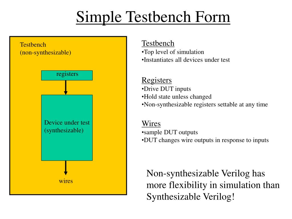
A crucial concept to grasp is how signals are declared inside the testbench:
- DUT Inputs are connected to variables of type
regin the testbench. This is because we need to actively assign and hold values onto these signals from within procedural blocks (like aninitialblock), which requires aregtype. - DUT Outputs are connected to variables of type
wirein the testbench. The testbench doesn't drive these signals; it passively observes the values being driven out by the DUT.
The following video explains this important distinction and shows how to instantiate the DUT.
Vivado Simulator and Test Bench in Verilog | Xilinx FPGA Programming Tutorials
This video, "Vivado Simulator and Test Bench in Verilog," clearly explains the declaration of signals and the instantiation of a DUT inside a testbench.
Watch these two short clips: Signal declarations: Pay close attention to the explanation of why inputs to the DUT are declared as reg and outputs as wire within the testbench. DUT instantiation: Observe how the DUT is instantiated, connecting its ports to the regs and wires you just declared.
2. Applying Inputs with Delays
To apply a sequence of inputs, we need two key Verilog features: a procedural block to contain our stimulus sequence and a way to control the timing between input changes.
initialblock: This is a procedural block where the code executes exactly once, starting at time 0 of the simulation. It's perfect for defining a finite sequence of test vectors.#delay operator: This operator pauses the simulation for a specified number of time units. For example,#10;creates a delay of 10 time units.timescaledirective: This compiler directive, placed at the top of a Verilog file, defines what a time unit means. For example,`timescale 1ns / 1pssets the main time unit to 1 nanosecond and the simulation precision to 1 picosecond.
The following reading provides a great summary of these concepts and puts them together in a complete example.
How to Write a Basic Verilog Testbench
This article from FPGA Tutorial clearly explains the essential constructs for writing a basic testbench.
Please read the following sections: Modelling Time in Verilog: Focus on the # delay operator and the timescale directive. Verilog initial block: Understand its purpose and syntax. Verilog Testbench Example: Read through the full example. Notice how it combines a module declaration, DUT instantiation, signal declarations, and an initial block with delays to apply a sequence of inputs.
Now, let's see this in action. The following video demonstrates how to write a simple testbench for a full adder, applying a few fixed input vectors one after another.
The video "WRITING VERILOG TEST BENCHES" provides a practical demonstration of applying a hard-coded stimulus sequence.
Watch the section showing a simple testbench for a full adder. Observe how the initial block is used to set the values of a, b, and c, with #5 delays in between each change.
3. Automating Stimulus Generation
Manually writing every single input combination, as we just saw, is manageable for a 3-input adder but quickly becomes impractical for designs with more inputs. A 16-bit input bus would require = 65,536 lines of code!
A more efficient method is to use a loop within the initial block to generate the stimulus programmatically. A for loop is perfect for iterating through all possible combinations of a set of inputs.
The same video you just watched demonstrates this improvement.
This next clip from "WRITING VERILOG TEST BENCHES" shows how to automate the stimulus generation for the same full adder.
Watch the section demonstrating the use of a for loop. Notice how it uses an integer i and concatenation {a,b,c} to efficiently apply all 8 possible input combinations. This is a much more scalable approach.
4. A Complete Example: Testbench for a 2:1 MUX
Let's consolidate everything we've learned by creating a testbench for a 2:1 multiplexer. In a previous module, you would have designed a MUX similar to the one below.
Design Under Test (DUT): mux_2_to_1.v
module mux_2_to_1 (
    input       a,
    input       b,
    input       sel,
    output      y
);

    assign y = sel ? b : a;

endmodule
Now, here is a complete testbench that instantiates this MUX and applies all possible input combinations using a for loop.
Testbench: tb_mux_2_to_1.v
`timescale 1ns / 1ps

module tb_mux_2_to_1();

    // 1. Declare signals to connect to the DUT
    // Inputs to DUT are 'reg'
    reg  tb_a;
    reg  tb_b;
    reg  tb_sel;

    // Outputs from DUT are 'wire'
    wire tb_y;

    // 2. Instantiate the Design Under Test (DUT)
    mux_2_to_1 dut (
        .a   (tb_a),
        .b   (tb_b),
        .sel (tb_sel),
        .y   (tb_y)
    );

    // 3. Apply stimulus sequence
    initial begin
        // Use $monitor to print values whenever a signal in the list changes
        $monitor("Time=%0t ns | sel=%b a=%b b=%b | y=%b", $time, tb_sel, tb_a, tb_b, tb_y);

        // Use a loop to generate all 8 input combinations
        // We can treat the inputs as a 3-bit vector {sel, b, a}
        for (integer i = 0; i < 8; i = i + 1) begin
            {tb_sel, tb_b, tb_a} = i;


            #10; // Wait 10 ns before applying the next input
        end


        #10; // Extra delay at the end
        $finish; // End the simulation
    end

endmodule
Analysis of the Testbench:
- Signal Declaration:
tb_a,tb_b, andtb_selareregtypes so theinitialblock can drive them.tb_yis awireto observe the MUX's output. - Instantiation: The
mux_2_to_1module is instantiated with the namedut, and its ports are connected to our testbench signals. - Stimulus Block:
- The
initialblock starts at time 0. $monitoris a system task that prints the specified message whenever any of its arguments (tb_sel,tb_a,tb_b,tb_y) change value. This is extremely useful for debugging.- The
forloop runs 8 times (for inputs). - In each iteration, the line
{tb_sel, tb_b, tb_a} = i;uses concatenation to assign the 3 bits of the integeridirectly to the three input signals. - The
#10;delay ensures that each input combination is held for 10 ns before the next one is applied, allowing us to see the result clearly in a simulation waveform. $finishis a system task that gracefully ends the simulation.
- The
When you run this simulation, the $monitor output would look something like this:
Time=0 ns   | sel=0 a=0 b=0 | y=0
Time=10 ns  | sel=0 a=1 b=0 | y=1
Time=20 ns  | sel=0 a=0 b=1 | y=0
Time=30 ns  | sel=0 a=1 b=1 | y=1
Time=40 ns  | sel=1 a=0 b=0 | y=0
Time=50 ns  | sel=1 a=1 b=0 | y=0
Time=60 ns  | sel=1 a=0 b=1 | y=1
Time=70 ns  | sel=1 a=1 b=1 | y=1
Conclusion
In this lesson, you took the crucial first step from verification theory to practice. You now have the fundamental tools to create a test environment and drive your designs with controlled input sequences.
Key Takeaways:
- A testbench is a non-synthesizable Verilog module used to simulate and verify a Design Under Test (DUT).
- In a testbench, signals connected to DUT inputs are declared as
reg, while signals connected to DUT outputs are declared aswire. - The
initialblock is used to define a sequence of actions that runs once at the beginning of a simulation. - The
timescaledirective and the#delay operator are used to control simulation timing, allowing you to apply inputs sequentially. - Using
forloops within aninitialblock is an efficient and scalable way to generate a comprehensive set of input vectors.
So far, we have been manually checking the output on the console or in a waveform viewer. This is not efficient for large designs. In the next lesson, we will enhance our testbench to do this checking automatically. You will learn how to create a self-checking testbench that compares the DUT's output against a pre-defined expected result and reports a pass or fail status.