Hello! Welcome back to our module on CPU and System Architecture.
In the last lesson, we built a foundational model of the cache hierarchy, understanding its structure with L1, L2, and L3 levels, and how data is organized into cache lines, sets, and ways. We established that L1 and L2 caches are typically private to a core, while the L3 cache is shared. This naturally leads to a critical question: what happens when multiple agents—like different CPU cores or a DMA controller—try to access the same memory?
This lesson dives into one of the most important topics in system architecture and a frequent subject of deep-dive interview questions: cache coherency.
Your learning goal for today is to: Analyze cache coherency issues in DMA and multi-core contexts, explaining why cache flush/invalidation is required.
We will cover:
- The fundamental problem of stale data when multiple bus masters are involved.
- How modern multi-core CPUs solve this with hardware coherency protocols like MESI.
- How embedded systems software must handle coherency for peripherals like DMA controllers.
- The critical role of memory barriers in ensuring the correctness of these operations.
The Core Problem: A Tale of Two Views
Cache coherency refers to the need to maintain a consistent, unified view of memory for all devices (or "bus masters") that can access it. When a CPU core has a private cache, its view of a memory location can diverge from the actual value in main memory (DRAM) or the view of another master.
This creates two classic failure scenarios, particularly in embedded systems using DMA. Let's examine a resource that illustrates this perfectly.
Managing Cache Coherency on Cortex-M7 Based MCUs
The application note 'Managing Cache Coherency on Cortex-M7 Based MCUs' from Microchip provides excellent diagrams of the two primary coherency problems with DMA.
Please read Section 3, 'Cache Coherency Issues' (pages 4-5). Focus on the two figures and their descriptions: Figure 3-1: DMA Writes to SRAM: This shows the DMA updating a buffer in main memory, but the CPU reads old, 'stale' data from its cache. Figure 3-2: DMA Reads from SRAM: This shows the CPU updating data in its write-back cache, but the DMA reads stale data from main memory because the cache hasn't been written back yet.
As you can see, without a mechanism to synchronize these views, the system is guaranteed to work with incorrect data. This problem exists in two primary contexts: between multiple CPU cores (a multi-core problem) and between a CPU and a peripheral (a DMA problem). Let's look at how each is solved.
Coherency in Multi-Core Systems: The Hardware Solution (MESI)
In a symmetric multi-processing (SMP) system, like the multi-core Intel and ARM processors you are targeting, the hardware provides an automatic solution. The processors use a cache coherency protocol to ensure that all cores maintain a consistent view of memory.
The most common protocol, and one you should be prepared to discuss in an interview, is MESI.
Intro to Cache Coherence in Symmetric Multi-Processor (SMP) Architectures
The video 'Intro to Cache Coherency in Symmetric Multi-Processor (SMP) Architectures' provides a good conceptual overview of the problem and introduces different protocol types.
Please watch the following segments: 00:00 - 02:35: This introduces the multi-core coherency problem. 04:00 - 06:54: This briefly explains directory-based protocols. You don't need to memorize this, but it's good for context. 09:12 - 14:15: This is the key part. It explains the MESI protocol and its four states. Pay close attention to the transitions between states as cores read and write data.
The core idea of MESI is that each cache line is tagged with one of four states. All the cache controllers "snoop" (monitor) the system bus for memory accesses. Based on what they see, they update the state of their own cache lines accordingly.

Here is a summary of the states:
- Modified (M): This is the only cached copy in the entire system. It has been modified by the local CPU, so the value in main memory is stale. Before another core can read this memory, this modified line must be written back to memory first.
- Exclusive (E): This is the only cached copy, and it is "clean" (identical to main memory). The core can write to this line locally without notifying other cores, at which point it transitions to Modified.
- Shared (S): Two or more cores have a copy of this cache line. All copies are clean. If one core wants to write to the line, it must first invalidate all other shared copies.
- Invalid (I): The data in this cache line is not valid. A read or write to this line will cause a cache miss.
In an SMP system, MESI or its variants (like MESIF or MOESI) provide hardware coherency, meaning you as the programmer typically don't have to manage it for core-to-core communication.
Coherency with DMA: The Software Solution
The situation changes when the other bus master is a DMA controller. Most DMA engines are not cache-coherent. They access main memory directly and are completely unaware of the CPU's caches or the MESI protocol.
This means the responsibility for maintaining coherency falls to you, the software engineer. This is a classic embedded systems challenge. The solution involves explicit cache maintenance operations.
Managing Cache Coherency on Cortex-M7 Based MCUs
Let's return to the Microchip application note, which details the software solution using CMSIS-standard functions for ARM Cortex-M processors. The principles are identical on higher-end ARM cores.
Read Section 4, 'Using Cache Maintenance APIs to Handle Cache Coherency' (pages 6-11). Pay close attention to: The distinction between Invalidate and Clean operations. The code example for DMA writes, which uses SCB_InvalidateDCache_by_Addr after the transfer. The code example for DMA reads, which uses SCB_CleanDCache_by_Addr before the transfer. The critical warning about buffer alignment and size.
Let's solidify the rules of thumb for software-managed coherency:
-
When DMA writes to memory (e.g., receiving data from a peripheral): The CPU's cache may hold stale data for that memory region.
- Solution: Before the CPU accesses the DMA buffer, you must invalidate the corresponding cache lines. This marks them as invalid and forces the CPU to fetch the fresh data from main memory on its next read.
- Sequence: DMA Transfer → DMA Interrupt → Invalidate Cache → CPU processes data.
-
When DMA reads from memory (e.g., transmitting data to a peripheral): The CPU may have updated the data in its write-back cache, but main memory still holds the old data.
- Solution: Before initiating the DMA transfer, you must clean (also known as flush) the corresponding cache lines. This forces any "dirty" lines to be written back to main memory.
- Sequence: CPU prepares data → Clean Cache → Start DMA Transfer.
A Critical Gotcha: Buffer Alignment
A common and difficult-to-debug error occurs when DMA buffers are not aligned to cache line boundaries.
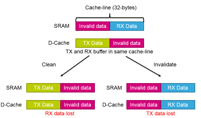
The rule is simple but vital: DMA buffers must be aligned to the cache line size, and their size should be a multiple of the cache line size. On most modern systems, this is 64 bytes. This prevents a cache maintenance operation on your DMA buffer from accidentally corrupting adjacent variables that happen to share the same cache line.
Ensuring Order: The Need for Memory Barriers
You might assume that writing Clean_Cache(); Start_DMA(); is sufficient. However, a high-performance, out-of-order CPU might reorder these operations for efficiency! It could speculatively start the DMA before the cache clean has fully completed, leading to the exact data corruption we are trying to avoid.
To prevent this, we need memory barriers. These are explicit instructions that tell the CPU and/or compiler not to reorder operations across the barrier.
Arm's Weakly-Ordered Memory Model and Barrier Requirements - Ash Wilding, Amazon
This is an advanced topic often explored in interviews at semiconductor companies. The video 'Arm's Weakly-Ordered Memory Model and Barrier Requirements' by Ash Wilding of Amazon provides an expert-level view, directly relevant to ARM-based SoCs from Qualcomm or Nvidia.
Watch the following segments about DMA and barriers: Coherent DMA (19:07 - 20:40): This explains why a barrier (DMB OSH ST) is needed to ensure the data is written to the buffer before the DMA transfer starts, even with a coherent DMA. Non-coherent DMA (20:40 - 22:28): This explains the interaction between a store and a cache clean instruction (DC CVAC). Notice that an explicit barrier isn't needed between these two specific instructions because of an address dependency, but a barrier is still needed relative to other operations like starting the DMA.
The key takeaway is that cache maintenance operations are memory accesses themselves. To guarantee that a cache clean completes before a write to a DMA control register, you must insert a proper memory barrier, such as a DSB (Data Synchronization Barrier) on ARM, between them.
Clean_Cache_Region(buffer);DSB(); // Ensures clean operation completesStart_DMA(buffer);
The Simple Alternative: Non-Cacheable Memory
Finally, there's another way to handle this: avoid the problem entirely. You can configure the system's Memory Protection Unit (MPU) or Memory Management Unit (MMU) to mark the memory regions used for DMA buffers as non-cacheable.
- Advantage: This is simple and safe. The software doesn't need to perform any cache maintenance because the CPU will always access that memory region directly from SRAM/DRAM.
- Disadvantage: Performance. You lose all the benefits of caching for those buffers. Every CPU access to the buffer will be a slow main memory access.
This is a classic engineering trade-off between performance and complexity. For control structures that are frequently accessed by both the CPU and DMA, but where performance is not paramount, making them non-cacheable is a common and robust design pattern. The Microchip PDF you reviewed earlier details this in its fifth section.
Conclusion
Understanding and correctly managing cache coherency is a hallmark of a senior embedded systems engineer. While hardware handles the complexity in multi-core CPU contexts, interaction with non-coherent peripherals like DMA puts the responsibility squarely on the software.
Key Takeaways:
- Coherency Problem: Multiple bus masters (CPUs, DMA) can have inconsistent views of memory, leading to data corruption from reading or writing stale data.
- Multi-Core Solution (Hardware): Snooping protocols like MESI automatically maintain coherency between CPU cores in an SMP system.
- DMA Solution (Software): For non-coherent DMA, the software must manually manage the cache:
- Invalidate cache after DMA writes to memory (so the CPU reads fresh data).
- Clean (Flush) cache before DMA reads from memory (so the DMA reads fresh data).
- Ordering is Crucial: Memory barriers (e.g.,
DMB,DSB) are required to prevent the CPU from reordering cache maintenance operations and memory-mapped I/O writes that trigger peripherals. - Alignment is Mandatory: DMA buffers must be aligned to cache line boundaries to prevent corruption of adjacent data.
- Alternative: Marking memory as non-cacheable via the MPU/MMU simplifies software at the cost of performance.
Preview of the Next Lesson:
We've now covered the cache and its coherency mechanisms. The next step up in the memory system is the Memory Management Unit (MMU). Our next lesson will be: Describe virtual-to-physical address translation via paging and the role of the TLB, analyzing the performance impact of misses. This is another cornerstone of modern OS and SoC architecture.