Hello! Welcome to the final lesson in our first module on the fundamentals of switched-mode power supplies.
In our last lesson, we explored inductor current ripple, treating our components—inductors, capacitors, and switches—as ideal, perfect elements. This was a useful simplification to understand the basic operation of a converter. However, the real world is not so tidy.
Today, we'll peel back that layer of idealization and confront the reality of parasitic capacitance and inductance. These are the unavoidable, often unwanted, electrical properties inherent in every physical component and printed circuit board (PCB) trace. Your goal is to be able to look at a power converter schematic or PCB layout and spot these hidden elements, because they are the root cause of many performance issues, including efficiency loss and electromagnetic noise. Understanding them is the first essential step toward understanding the problem that Zero Voltage Switching (ZVS) is designed to solve.
What Are Parasitics?
In the simplest terms, parasitics are the unintentional resistances, inductances, and capacitances that exist in a physical circuit. You don't add a "parasitic inductor" to your schematic, but the physical wire or trace you use to connect components has inductance all the same.
Let's start with a quick video that defines this concept clearly.
This video from Altium Academy provides a concise definition of parasitics and explains how they arise from the physical nature of electronic systems.
Please watch from 0:29 to 1:40. Focus on the core idea that parasitics are unintentional circuit elements that you didn't explicitly design for, but exist due to the physical layout.
Where Do Parasitics Come From?
Parasitics aren't just random annoyances; they arise from fundamental physical principles and can be found in two main places: within the components themselves and in the PCB layout that connects them.
1. Parasitics within Components
No real-world component is pure. A capacitor isn't just a capacitor; it's a complex network of ideal and parasitic elements.
Switches (MOSFETs):
As the heart of a switching converter, the MOSFET is a major source of parasitics.
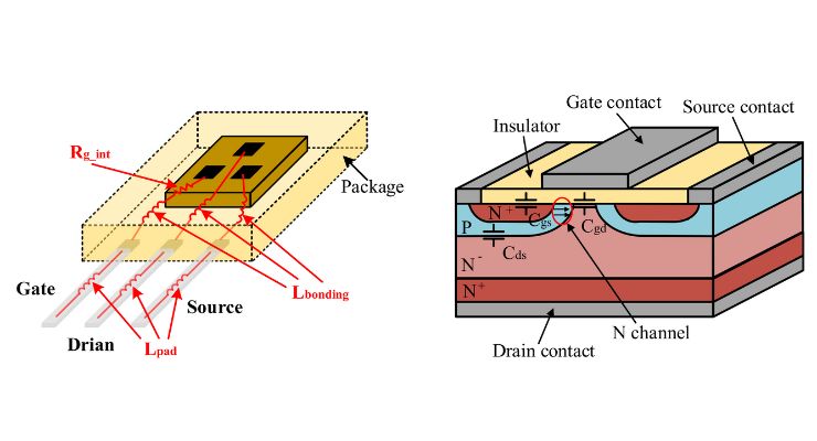
- Internal Capacitances: Due to its physical structure, a MOSFET has inherent capacitances:
- (Gate-Source): Must be charged to turn the device on.
- (Drain-Source): Also called output capacitance (). This capacitance must be charged and discharged every switching cycle, which is a major source of switching loss. We will focus heavily on this in the next module.
- (Gate-Drain): Also known as the "Miller capacitance." It couples the output back to the input and significantly affects switching speed.
- Package Inductances: The leads, pads, and internal bonding wires of the component package all have small but significant inductances. The inductance in the source connection, often called common source inductance, is particularly important because it is shared between the power path and the gate drive loop, which can slow down switching and increase losses.
Capacitors and Inductors:
Like MOSFETs, passive components also have parasitic elements.
Let's return to the Altium Academy video, which does a great job of showing the parasitic models for real-world capacitors and inductors.
Watch from 8:14 to 10:28. Pay attention to the equivalent circuit models for a capacitor (which includes Equivalent Series Resistance - ESR, and Equivalent Series Inductance - ESL) and an inductor (which includes winding capacitance and DC resistance).
2. Parasitics in the PCB Layout
The way you arrange components on a PCB is just as important as the components themselves. The traces, planes, and vias that connect everything create their own network of parasitic elements.
Parasitic Inductance and the Concept of Loop Area
Anytime current flows in a closed loop, that loop has inductance. The single most important principle for you to remember when reviewing a PCB layout is:
Inductance is proportional to the area of the current loop.
A large loop formed by a power trace and its ground return path will have high parasitic inductance. A small, tight loop will have low parasitic inductance. This is the foundation of high-frequency power layout.
The following video provides an excellent and intuitive demonstration of this principle.
Inductance in PCB Layout: The Good, the Bad, and the Fugly
This video from HACKADAY visually explains why the physical area enclosed by a current path is the dominant factor in creating parasitic inductance.
Watch from 12:50 to 15:00. The key takeaway is the comparison between two wire configurations: the one forming a large loop has more inductance than the one where the wires are kept close together.
Parasitic Capacitance
Any two conductive surfaces separated by an insulator (like the PCB's fiberglass material) form a capacitor. This can occur between:
- Two adjacent traces on the same layer.
- A trace on one layer and a ground or power plane on another layer.
- The large power and ground planes themselves.
The Altium video also gives clear examples of how PCB features create parasitic capacitance.
Watch from 3:41 to 7:00. This section explains plane capacitance, capacitance between copper pours and traces, and also introduces the concept of via inductance.
Why Parasitics Matter: The "Hot Loop"
Now that we know what parasitics are and where they come from, why should we care?
In a switching converter, currents change extremely rapidly (high ). Because of the relationship , even a tiny parasitic inductance () can create large, damaging voltage spikes. These spikes cause electromagnetic interference (EMI) and stress components. Furthermore, the energy stored in these parasitic inductances and capacitances gets dissipated as heat (often in parasitic resistances), which reduces the converter's efficiency.
To manage this, designers focus on the "hot loop"—the part of the circuit with the fastest-switching currents. In a buck converter, this loop consists of the input capacitor, the top switch, and the bottom switch (or diode).
How to Minimize Parasitics in Switching Power Supplies
This article from DigiKey provides a fantastic, practical overview of the hot loop and how layout choices directly impact parasitic inductance and converter performance.
Please read the section 'Fundamentals of switching power supply hot loops'. Focus on Figure 2, which clearly shows the physical components of the hot loop and labels the parasitic ESL (inductance) and ESR (resistance) within it.
The energy stored in the parasitic inductance () of this hot loop causes voltage ringing, and this energy is then burned off as heat by the parasitic resistance (), creating switching losses.
Practical Impact: Minimizing Parasitics Through Layout
Your goal is to review and optimize PCBs, and this is where these concepts become tools. A "good" layout is one that minimizes the area of the critical hot loops.
The DigiKey article provides a perfect case study comparing three different layouts for the same buck converter. By changing only the placement of the input capacitor, the parasitic inductance of the hot loop is dramatically altered, leading to measurable differences in efficiency and voltage ripple.
How to Minimize Parasitics in Switching Power Supplies
Let's continue with the DigiKey article to see a real-world example of layout optimization.
Read the sections 'Minimizing parasitic parameters with component placement' and 'Minimizing parasitic parameters for discrete components'. Study Figures 4, 5, and 6 to see the different layouts, and then look at the results in Figures 7 and 8. Notice how 'Vertical Hot Loop 1', with the shortest current path, has the lowest parasitics and best performance.
This case study demonstrates the core principle in action: placing critical components as close together as possible to minimize loop area reduces parasitic inductance, which in turn improves efficiency and reduces noise. This is a key pattern to look for during a PCB review.
Test your understanding!
Below are two simplified layouts for the hot loop of a buck converter. The loop consists of the input capacitor (Cin), the high-side MOSFET (Q1), and the low-side MOSFET (Q2). The current flows from Cin, through Q1 and Q2, and returns to Cin's ground.
Layout A:
+-------+      +----+      +----+
|       |------| Q1 |------| Q2 |
|  Cin  |      +----+      +----+
|       |-------------------------|
+-------+                         |
   |                              |
  GND ----------------------------+
Layout B:
+-------+   +----+
|       |---| Q1 |
|  Cin  |   +----+
|       |   +----+
+-------+---| Q2 |
   |        +----+
  GND
(Imagine Q1 is placed directly on top of Q2 in a 3D sense, or very close side-by-side, sharing a common ground connection with Cin)
Which layout is better for a high-frequency switching converter, and why?
Show answer
Layout B is significantly better.
The reason is that it creates a much smaller, tighter hot loop. The physical area enclosed by the current path (from Cin+, through Q1, through Q2, and back to Cin-) is minimized.
According to the principle we've discussed, smaller loop area leads to lower parasitic inductance. Lower inductance in the hot loop will result in smaller voltage spikes, less ringing, lower EMI, and higher efficiency.
Layout A creates a long, wide loop, which maximizes parasitic inductance and would lead to poor performance in a real-world design.
Conclusion
This lesson completes our tour of the fundamental building blocks of switching converters. We've moved from ideal components to the messy reality of parasitics.
Key Takeaways:
- Real-world components and PCB layouts contain parasitic resistance, inductance, and capacitance.
- Component Parasitics: Switches have internal capacitances () and package inductance. Capacitors have ESR and ESL.
- Layout Parasitics: The most critical is loop inductance, which is proportional to the physical area enclosed by a current path.
- These parasitics are the primary cause of voltage spikes, ringing, EMI, and switching losses.
- A key goal of PCB layout for power converters is to minimize the area of high-current "hot loops" to reduce parasitic inductance.
Now that we understand what parasitics are and the problems they cause, we are ready to quantify their impact. In the next module, we will begin our investigation of The Hard Switching Problem. Our first lesson will explain exactly how the interplay of current, voltage, and these parasitic elements creates significant power loss during the switching transitions. This will lay the final piece of groundwork before we can truly appreciate the solution: Zero Voltage Switching.