Hello! Welcome to the first lesson in our new module on PCB layout principles for ZVS converters.
In our last lesson, we concluded our tour of ZVS topologies by examining their common failure modes. We saw how loss of ZVS at light loads and, more critically, the reverse recovery behavior of MOSFET body diodes can lead to catastrophic failure. You learned that these destructive events are often triggered by the unavoidable parasitic inductances and capacitances within the circuit.
Today, we begin to tackle this problem head-on. If parasitics are the enemy, then careful PCB layout is our primary weapon. This lesson focuses on the single most sensitive part of a high-frequency converter's layout, addressing the learning outcome: Identify critical layout considerations for minimizing inductance in high-frequency gate drive loops. Mastering this is the first and most crucial step toward designing robust and reliable power electronics.
1. Why the Gate Drive Loop is So Critical
In an ideal world, the voltage signal from the gate driver would appear instantly and perfectly at the MOSFET's gate. In reality, every millimeter of PCB trace adds parasitic inductance and resistance, which can corrupt this signal.
The core of the problem lies in the fundamental relationship for an inductor:
To switch a MOSFET quickly, the gate driver must source or sink a large current () in a very short time (). This creates an extremely high rate of change of current (). Even a tiny amount of parasitic inductance () in the gate drive path can result in a significant voltage drop or spike () across that inductance.
Let's consider a practical example. A modern gate driver might source 2 Amps of current in 5 nanoseconds. If the gate drive loop has just 5 nanohenries (5 nH) of parasitic inductance—a very plausible amount in a mediocre layout—the induced voltage drop is:
If you're using a 5V gate drive, this parasitic voltage drop consumes 40% of your drive voltage! This has several dangerous consequences:
- Slower Switching: The reduced voltage at the gate slows down the MOSFET's turn-on, increasing switching losses.
- Ringing and Overshoot: The parasitic inductance forms a resonant RLC circuit with the MOSFET's gate capacitance. This can cause the gate voltage to ring, potentially exceeding the MOSFET's maximum rating.
- Spurious Turn-On (Shoot-through): If noise or ringing on the gate signal crosses the MOSFET's threshold voltage (), it can turn on when it's supposed to be off. In a half-bridge, this causes a direct short-circuit from the input voltage to ground through both transistors—the destructive "shoot-through" we discussed in the last lesson.
The following video provides an excellent introduction to how these parasitic elements in a PCB layout can corrupt the clean signals we need for reliable switching.
Basics of grounding and bypassing in power electronics PCB layout
Watch this segment from a video by Prof. Sam Ben-Yaakov to see a visual explanation of how parasitic inductance in PCB traces can turn a clean PWM signal into a noisy, unreliable mess at the MOSFET gate.
Please watch the video from the beginning to 04:57. Focus on how the seemingly small impedance of copper traces, when combined with high-frequency currents, creates potential differences that corrupt the gate drive signal and can lead to device malfunction or failure.
2. The Golden Rule: Minimize Loop Area
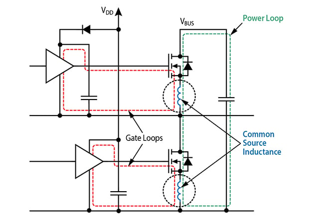
To minimize parasitic inductance, you must minimize the physical area of the current loop. The gate drive loop consists of the complete path the current takes from the gate driver, through the MOSFET's gate, and back from the MOSFET's source to the gate driver's ground/return terminal.
The inductance of a rectangular loop is a function of its length and the distance between the forward and return paths. To make the inductance small, we need to make that loop area as small as possible.
The following video explains the physics behind this principle and introduces the most important concept for achieving a low-inductance layout.
This video from OMICRON Lab, titled "PCB Layout Fundamentals," breaks down the physics of loop inductance. It explains why minimizing loop area is key and how high-frequency currents behave in a way that helps us achieve this.
Please watch from 06:01 to 16:41. The first part (until 14:04) explains why a smaller loop area leads to lower inductance and better magnetic field cancellation. The second part (starting at 14:04) introduces the crucial concept that high-frequency current follows the path of least inductance, not least resistance, automatically flowing under the forward trace if a return plane is available.
The key takeaways from the video are:
- Inductance is proportional to loop area. A long, narrow loop has much lower inductance than a short, wide one.
- High-frequency currents take the path of least inductance. This means the return current will naturally try to flow directly underneath the outgoing current path to minimize the loop area.
This leads us to the single most effective technique for minimizing gate loop inductance: the vertical loop. Instead of routing the gate signal and its return path side-by-side on the same layer (a lateral loop), we route the gate signal on one layer and provide a solid copper plane for the return current on an adjacent layer. The loop area is now determined by the trace length multiplied by the very small vertical distance between the PCB layers, dramatically reducing inductance.
3. Practical Techniques for an Optimized Gate Drive Layout
Knowing the principles is one thing; applying them is another. Here are the critical techniques you should look for when reviewing a gate drive layout on a PCB.
Component Placement and Bypass Capacitors
The first step is to place the gate driver IC as close as possible to the MOSFET it is driving. This makes the traces shorter, which directly reduces loop area.
Next, a local bypass capacitor must be placed right at the driver's supply pins. This capacitor acts as a local, low-impedance reservoir of charge for the gate. It ensures the high-frequency gate current circulates in a very small loop between the capacitor, the driver, and the MOSFET, instead of traveling all the way back to the main power supply.
Basics of grounding and bypassing in power electronics PCB layout
Let's revisit Prof. Ben-Yaakov's video to understand the role of the bypass capacitor.
Please watch the segment from 21:07 to 24:26. It explains why a bypass capacitor is needed to provide a local, low-impedance path for high-frequency currents and discusses why small ceramic capacitors are preferred.
The Kelvin Connection: Separating Power and Control
One of the most insidious problems is "common source inductance." The MOSFET source connection is part of both the high-current power loop and the sensitive gate drive loop. As the high power current switches, it creates a large voltage spike across the source's parasitic inductance. If the gate driver's return is connected to this "noisy" point, that voltage spike is directly injected into the gate drive signal, corrupting it.
The solution is a Kelvin connection. This means providing a dedicated, separate trace from the MOSFET source pin directly back to the gate driver's return pin, completely separate from the high-current power path.
PCB Layout Rules for Converters and Motor Drives
This presentation from EPC provides clear, concise slides on PCB layout rules. The following sections will visually explain the impact of gate loop inductance and how to implement a Kelvin connection.
Please review slides 6, 12, and 13. Slide 6 (Impact of Gate Loop Inductance): Note how it identifies separate turn-on and turn-off loops and the need for a resistor to damp ringing. Slide 12 (What About the Gate Connection): This shows the ideal vertical loop structure, with a gate drive track on one layer and a return polygon on the next. Slide 13 (To Kelvin or not to Kelvin?): This introduces the concept of a Kelvin connection by separating the gate return from the main source connection.
Test your understanding!
You are reviewing a PCB layout for a half-bridge converter. You see two different layout approaches for the gate drive circuit of the low-side MOSFET.
- Layout A: The gate driver IC is on the top layer. A 10mm long, 0.2mm wide trace goes from the driver to the MOSFET gate. The return current travels back to the driver on another 0.2mm wide trace on the same layer, running parallel to the first trace but 3mm away.
- Layout B: The gate driver IC is also on the top layer with an identical 10mm trace to the gate. However, the return path is a solid copper plane on layer 2, which is 0.15mm directly below the top layer.
Which layout provides lower gate loop inductance, and why?
Show answer
Layout B provides significantly lower inductance.
The inductance is proportional to the area of the current loop.
- In Layout A (a lateral loop), the area is approximately the trace length multiplied by the lateral separation: .
- In Layout B (a vertical loop), the area is the trace length multiplied by the vertical separation between layers: .
By using an adjacent layer for the return path, Layout B reduces the loop area by a factor of 20, resulting in a much lower and superior gate loop inductance.
Conclusion
In this lesson, you have learned why minimizing the parasitic inductance of the gate drive loop is paramount for the performance and reliability of any high-frequency switched-mode power supply.
Key Takeaways:
- High is the challenge: The fast currents required to drive a MOSFET gate make the circuit extremely sensitive to even nanohenries of parasitic inductance.
- Minimize Loop Area: The primary strategy for reducing inductance is to minimize the physical area of the gate drive current loop.
- Use Vertical Loops: The most effective way to minimize loop area is to route the gate signal on one layer and its return path on an adjacent, parallel layer.
- Place Components Strategically: Keep the gate driver, bypass capacitor, and MOSFET as close to each other as possible.
- Isolate with Kelvin Connections: Use a dedicated Kelvin connection for the gate driver's return to prevent noise from the high-current power path from corrupting the gate signal.
You can now recognize the features of a well-designed gate drive circuit on a PCB. In our next lesson, we will shift our focus from the sensitive, low-power gate loop to the brute-force, high-current power loop. We will explore how to apply these same principles to minimize inductance in the paths that carry the full load current, which is critical for managing voltage overshoot and EMI.