Hello! Welcome to the final lesson in our module on practical ZVS design and optimization.
In the previous lesson, we conducted a detailed comparison of the Active Clamp Flyback, Phase-Shifted Full-Bridge, and LLC converters. You learned how to evaluate them based on efficiency, power density, complexity, and cost. This gave you the "why" behind choosing a specific topology for an application.
Today, we address the critical learning outcome: Recognize common failure modes in ZVS operation, such as loss of ZVS and component overstress. While ZVS topologies offer incredible performance, they are not foolproof. Understanding their unique failure mechanisms is essential for your goal of reviewing and optimizing PCBs, as it allows you to spot designs that might be living on the edge of reliability.
1. The Fragility of "Soft" Switching
ZVS is often portrayed as a perfect solution to switching losses, but the reality is more nuanced. The "soft" switching condition is not guaranteed; it can be lost if the converter operates outside its intended design window. This leads to two main categories of failure:
- Loss of ZVS: The converter reverts to hard switching, leading to high losses and thermal stress.
- Component Overstress: Even when ZVS is achieved, the underlying mechanism can stress components—particularly the MOSFET's body diode—in subtle but destructive ways.
Let's investigate these two failure modes in detail.
2. Failure Mode 1: Losing the "Zero"
Almost all soft-switching topologies have operating regimes where the conditions for ZVS are no longer met.
Beware of Zero Voltage Switching
This application note from Vishay, titled "Beware of Zero Voltage Switching," provides an excellent high-level overview of this problem. It's a good reminder that ZVS isn't a silver bullet.
Please read the short section that begins with "Almost all soft switching topologies have potential operating regimes where ZVS is lost." This is typically found on page 3. Focus on understanding the primary cause (light load) and the consequence (reverting to hard commutation).
As the reading highlights, the most common reason for losing ZVS is light load operation. In many topologies, like the PSFB's lagging leg, the energy stored in the primary current is used to discharge the switch's output capacitance () to achieve ZVS. At light loads, there simply isn't enough current—and therefore not enough energy—to fully discharge this capacitance before the switch turns on.
Consequences of Losing ZVS:
- Reverts to Hard Switching: The MOSFET turns on while there is still significant voltage across it, causing the exact turn-on switching losses we sought to eliminate.
- Increased Thermal Stress: The sudden re-appearance of switching losses generates heat that the thermal design may not be prepared for, potentially damaging the switch.
- Change in Commutation: As the reading notes, the body diodes can suddenly shift from a gentle soft commutation to a stressful hard commutation, which we will discuss next.
Example: The LLC Converter Under Overload
A fascinating example occurs in LLC converters, but under overload conditions. The control system increases the switching frequency to regulate the output, which can push the converter's operating point from the desirable ZVS region into the dangerous ZCS (Zero Current Switching) region.
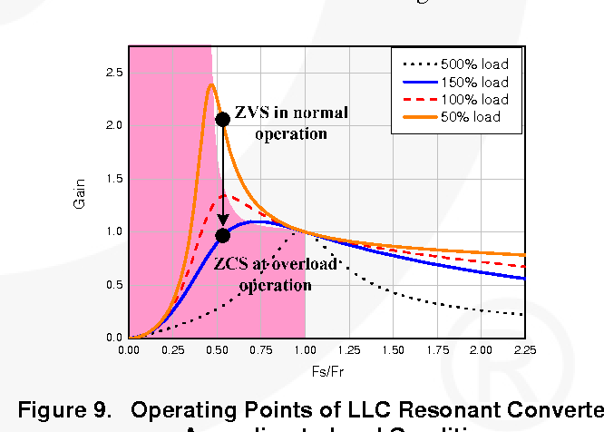
Let's watch a quick video that explains why this region is so dangerous.
How LLC Resonant Converter Works
We've seen this video before, but its explanation of the LLC's operating regions is worth revisiting now that we're focused on failure modes.
Please re-watch the segment from 10:19 to 11:34. The narrator describes what happens when the operating frequency goes below the peak gain, entering the "capacitive region." Pay close attention to the consequences he lists: loss of ZVS, hard switching, reverse recovery loss, shoot-through, and potential MOSFET failure.
This brings us to the most critical and subtle failure mechanism in ZVS converters: the behavior of the MOSFET body diode.
3. Failure Mode 2: The Body Diode's Revenge
In any circuit that achieves full ZVS, the MOSFET's intrinsic body diode must conduct during the dead time. This is what allows the voltage across the switch to drop to zero before turn-on. However, this reliance on the body diode is the source of a major reliability risk.
The problem is that the body diodes integrated into most standard MOSFETs are not high-performance rectifiers. They are slow and have a high reverse recovery charge ().
The Peril of Reverse Recovery
When a diode switches from conducting forward current to blocking reverse voltage, it doesn't happen instantly. For a brief period, stored charge carriers allow a large current to flow in the reverse direction. This is the reverse recovery current ().
When this happens in a half-bridge or full-bridge, the consequences can be catastrophic.
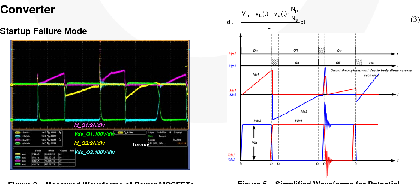
This shoot-through current leads to:
- Massive losses and extreme thermal stress.
- High and , generating significant EMI.
- Destruction of the MOSFET.
The following reading explains the physics behind this destructive failure.
Analysis of MOSFET Failure Modes in LLC Resonant ...
This excellent application note from ON Semiconductor, "Analysis of MOSFET Failure Modes in LLC Resonant Converter," dives deep into the physical mechanism of device failure. It's a bit dense, but it perfectly explains how reverse recovery leads to destruction.
Please read the sections "Body Diode Reverse Recovery dv/dt" and "Breakdown dv/dt" (pages 7-9). Focus on understanding how the reverse recovery current (I_rr) flowing through the internal base resistance (R_b) can trigger the parasitic BJT, leading to latch-up and device failure. The diagrams in this section are very helpful.
The key takeaway is that the large reverse recovery current can activate a parasitic BJT inherent in the MOSFET's structure. Once this BJT turns on, it creates a localized hot spot that leads to thermal runaway (latch-up), irreversibly destroying the device.
4. Failure in Action: LLC Converter Corner Cases
The LLC converter is a high-performance topology, but it's particularly vulnerable to body diode issues during transient events like startup and overload.
Analysis of MOSFET Failure Modes in LLC Resonant ...
Let's return to the ON Semi application note to see how these failures manifest in a real-world scenario.
Please read the sections "Startup Failure Mode" (pages 2-3) and "Overload Failure Mode" (pages 4-5). In the startup section, notice how empty output capacitors cause an unusually large resonant current, which leads to more stored charge in the body diode and a massive shoot-through spike. In the overload section, connect the explanation back to what we discussed earlier: the operating point shifts into the ZCS region, causing severe reverse-recovery stress.
These examples show that a converter that is perfectly stable in steady-state can be destroyed by a predictable transient event if the designer hasn't accounted for these failure modes.
Test your understanding!
You are reviewing the schematic for a new high-density 400W LLC power supply. You notice the designer has used standard, low-cost MOSFETs. What potential reliability concern does this raise, and what would you look for in the MOSFET's datasheet to either confirm or alleviate your concern?
Show answer
The use of standard MOSFETs in a high-performance LLC converter is a potential red flag. The primary concern is the poor reverse recovery performance of their intrinsic body diodes. This could make the converter susceptible to destructive shoot-through currents during startup, overload, or other transient conditions.
To investigate, you should look for the Reverse Recovery Charge () and Reverse Recovery Time () specifications in the MOSFET datasheet. A high (often in the hundreds or thousands of nanocoulombs for high-voltage devices) would confirm the risk. Ideally, for this application, you would want to see a MOSFET specifically marketed as having a "fast recovery" or "low " body diode. The absence of such a feature on a standard MOSFET is a significant reliability risk in a ZVS topology.
Conclusion
You now understand that the elegance of Zero Voltage Switching comes with hidden dangers. Achieving high reliability is not just about enabling ZVS, but also about preventing its loss and managing its consequences.
Key Takeaways:
- ZVS can be lost, most commonly at light loads, causing the converter to revert to hard switching with high thermal stress.
- The MOSFET body diode is the Achilles' heel of many ZVS topologies. Its conduction is necessary for ZVS, but its poor reverse recovery () performance can lead to destructive shoot-through currents.
- Transient events are critical. Startup, overload, and short-circuit conditions often create the worst-case stress on the body diodes and are common triggers for failure.
- Component selection is paramount. Using MOSFETs with integrated fast-recovery body diodes (low ) is a key strategy for mitigating these failure modes, even if it comes at a higher cost.
This lesson concludes our module on the practical design and optimization of ZVS converters. You've journeyed from selecting components to comparing topologies and now to identifying their failure modes.
In our next and final module, PCB Layout Principles for ZVS Converters, we will explore how the physical arrangement of components on the circuit board is critical to managing the parasitic effects that cause these failures. A good layout is the final, essential step in building a reliable and efficient ZVS power supply.