Hello! Welcome back to our module on PCB layout principles.
In the last lesson, we focused on the high-frequency gate drive loop. You learned that due to the extremely high rate-of-change of current () needed to switch a MOSFET quickly, minimizing the parasitic inductance of the gate loop is critical to prevent signal degradation, ringing, and spurious turn-on. The key strategies were minimizing loop area, using vertical loops with adjacent return planes, and employing Kelvin connections.
Today, we apply these same fundamental principles to a different, and in many ways more challenging, part of the circuit. This lesson will address the learning outcome: Identify critical layout considerations for minimizing parasitic inductance in high-current power loops. We'll explore why the paths carrying the full converter current are a major source of performance degradation and EMI, and how to design them for optimal performance. For your goal of reviewing and optimizing PCBs, this is where you'll find some of the most significant opportunities for improvement.
1. Identifying the Critical Power Loops
Every switching converter has several current paths, but not all are created equal. The paths that carry high-frequency, high-magnitude AC currents are the most critical from a layout perspective. These are often called "hot loops" because they contain high and noise and are major sources of EMI and switching losses.
Let's use the familiar buck converter as our example to identify these loops.
(Sponsored) Switching Regulator PCB Design - Phil's Lab #60
This video from Phil's Lab provides a clear breakdown of the different current loops in a buck converter. Pay close attention to which loops he identifies as the high-frequency switching loops.
Please watch from 04:40 to 06:00. The video will distinguish between the input and output loops, which carry mostly DC, and the two high-frequency loops that are active when the switch is ON and OFF.
As the video explained, in a buck converter, the most critical loop is the one formed by the input capacitor, the high-side switch, and the low-side switch (or diode). When the high-side switch turns on, current flows from the capacitor through the switch. When it turns off and the low-side switch turns on, the current path changes. The key insight is that the path connecting these three components sees the full input current rapidly turning on and off. This is the "hot loop."
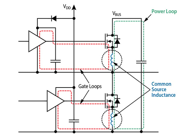
In this half-bridge schematic, which is the core of a synchronous buck converter, the main high-current power loop is shown by the green dashed line. It flows from the input capacitor (not shown, but connected to VBUS and GND), through the top MOSFET (Q_HS), the bottom MOSFET (Q_LS), and back to the capacitor's ground. Minimizing the inductance of this loop is our primary goal.
2. Why Power Loop Inductance Matters
The core principle is the same one we saw for gate loops: inductance is proportional to the physical area enclosed by the current path.
However, the consequences of inductance in the power loop are magnified because the current () is much larger than in the gate loop.
Let's explore this fundamental concept and its consequences.
Inductance in PCB Layout: The Good, the Bad, and the Fugly
This HACKADAY video, "Inductance in PCB Layout," offers an excellent, intuitive explanation of why loop area is the dominant factor in a trace's inductance. It perfectly illustrates the concept of magnetic field cancellation.
Please watch two segments: 12:57 to 15:12: This part visually demonstrates that a larger loop has more inductance and introduces the core idea that bringing the supply and return paths close together causes their magnetic fields to cancel, reducing inductance. 23:04 to 24:21: This is a great summary that reinforces the main takeaway: larger loop area means higher inductance, which means higher impedance and a 'dirtier' power supply.
High inductance in the power loop has three major negative effects:
- Voltage Overshoot and Ringing: The large of the switching current flowing through the loop inductance () creates significant voltage spikes: . This can easily exceed the voltage rating of your MOSFETs, leading to failure.
- Power Loss: The energy stored in this parasitic inductance () must be dissipated in every switching cycle, primarily as heat in the switches and parasitic resistances. This directly reduces converter efficiency.
- Electromagnetic Interference (EMI): A large, high-current loop is an extremely effective antenna. It radiates electromagnetic energy, which can interfere with other electronics and cause a product to fail mandatory EMC (electromagnetic compatibility) testing.
The following document from EPC, a leader in GaN technology, powerfully illustrates these effects. Even if you're working with standard silicon MOSFETs, the principles are identical.
In this white paper, "Optimizing PCB Layout," look at Figure 3 to see the real-world impact of power loop inductance.
Please read the introduction on page 2, focusing on the section that discusses Figure 3. Notice how a small increase in loop inductance (from 0.4 nH to 2.9 nH) causes a significant drop in efficiency and a dramatic increase in voltage overshoot on the switching node.
3. Practical Layout Strategies
Now that we understand the 'why', let's focus on the 'how'. The goal is to make the physical area of the hot loop as small as humanly possible.
Strategy 1: Smart Component Placement
The first and most important step is to place the components of the hot loop as close together as possible. For a buck converter, this means the input bypass capacitor(s) and the high-side and low-side MOSFETs must be tightly clustered.
(Sponsored) Switching Regulator PCB Design - Phil's Lab #60
Let's return to the Phil's Lab video. This segment demonstrates the practical process of placing components to minimize loop areas.
Watch from 06:00 to 08:38 and 10:46 to 15:09. The first segment covers the general principles. The second segment shows the actual placement in a PCB tool. Focus on the rationale for placing the input capacitor right next to the switching IC to create the tightest possible input loop.
Strategy 2: Using PCB Layers for Field Cancellation
This is the most powerful technique and directly builds on what we learned in the last lesson. We can minimize loop area by creating a "vertical loop" where the forward current path and the return current path are on adjacent PCB layers.
The resources from Analog Devices and EPC provide excellent comparisons of different layout philosophies.
How to Optimize Switching Power Supply Layout by ...
This article from Analog Devices and the EPC paper you saw earlier both compare different ways to arrange the power loop using PCB layers. They introduce the concepts of 'lateral' and 'vertical' loops.
Please read the section "Hot Loop PCB ESR and ESL vs. Decoupling Capacitor Position." It compares a 'vertical loop' (capacitor on the bottom layer) with a 'horizontal loop' (capacitor on the top layer). Notice in Figure 5 how the vertical loop yields higher efficiency and lower input ripple, confirming it has lower inductance and resistance.
The EPC paper (LINK) takes this analysis a step further, providing a detailed breakdown of three common approaches.
- Lateral Power Loop: Components are on the top layer. The current flows out and back on the same layer. This creates a relatively large loop area. It can be improved by placing a solid ground plane on an adjacent layer to act as a "shield," but it's not the most effective method. (See Figure 4 in the EPC paper).
- Vertical Power Loop: The input capacitors are placed on the bottom side of the PCB, directly under the switches on the top side. The current travels down through vias to the capacitor and back up through other vias. The opposing currents on the top and bottom layers provide excellent magnetic field self-cancellation. The loop inductance is primarily determined by the thickness of the PCB. (See Figure 5 in the EPC paper).
- Optimal Power Loop: This is the best-in-class approach. It keeps all components on the top side but uses the adjacent inner layer (e.g., Layer 2) as the dedicated return path for the hot loop current. The current flows out on Layer 1 and immediately returns on Layer 2, directly underneath. This creates the smallest possible loop area, combines field self-cancellation, and is independent of the total board thickness. (See Figure 6 in the EPC paper).
When reviewing a PCB, look for this optimal structure: input capacitors right next to the switches, with a solid, uninterrupted copper plane on the layer immediately below, serving as the return path.
Strategy 3: Ground Planes and Vias
A continuous ground plane is your best friend. As we've learned, high-frequency return currents naturally follow the path of least inductance, meaning they flow directly under the forward trace.
- Avoid Cuts and Slots: Any break, slot, or cutout in the ground plane under a high-current trace forces the return current to make a detour. This dramatically increases the loop area and, therefore, the inductance.

*This image shows parasitic inductances in a full-bridge converter. Elements like L1, L2, L7, and L8 represent the inductance of the copper traces forming the power loops. The goal of a good layout is to minimize these values by minimizing the area of the loops they are part of.*
- Use Vias Correctly: Vias are necessary to connect different layers, but each via adds inductance and resistance. For high-current paths:
- Use multiple vias in parallel to reduce the total inductance and resistance.
- Place these vias as close as possible to the component pads (e.g., the capacitor pads and the MOSFET source pad). Vias scattered far away from the current path are ineffective.
How to Optimize Switching Power Supply Layout by ...
The Analog Devices article provides a great analysis of via placement.
Read the final section, "Hot Loop PCB ESR and ESL vs. Via Placement." The key takeaway from Table 3 is that adding vias helps, but the vias placed closest to the component pads provide the vast majority of the benefit.
Test your understanding!
You are reviewing a PCB for a 12V input buck converter. You see two potential layouts for the input stage "hot loop."
- Layout A: The input ceramic capacitor is placed 20mm away from the half-bridge switches. The connection is made with wide traces on the top layer, and the ground return uses a shared ground plane.
- Layout B: The input ceramic capacitor is placed immediately adjacent to the half-bridge switches (<2mm away). The ground pads of the capacitor and the low-side MOSFET source are connected with a small copper area on the top layer, which is then connected to the main ground plane with multiple vias. The positive terminal of the capacitor connects directly to the high-side MOSFET drain.
Which layout is better for minimizing parasitic inductance, and why? Referencing at least two of the strategies discussed.
Show answer
Layout B is vastly superior.
-
Smart Component Placement: Layout B places the critical hot loop components (capacitor and switches) as close together as possible. This is the first and most important rule for minimizing the physical size of the loop, directly applying Strategy 1. Layout A creates a large loop by placing the capacitor far away.
-
Using Vias Correctly / Small Loop Area: Layout B creates a very small, local loop on the top layer and uses multiple vias right at the loop's ground node to connect to the main plane. This follows the principles of Strategy 3. The total loop area—out from the cap, through the switches, and back to the cap's ground—is minimized. In Layout A, the current has to travel 20mm out and 20mm back, creating a large and inductive loop that will act as an efficient antenna for EMI.
Conclusion
In this lesson, we've extended our understanding of parasitic inductance from the gate drive circuit to the high-current power loop. You can now identify the most critical "hot loops" in a converter and recognize the key layout techniques used to control them.
Key Takeaways:
- Identify the Hot Loop: The most critical loop is the one carrying high-magnitude, high-frequency AC current, typically involving the input capacitor and the main switches.
- Minimize Loop Area: The fundamental goal is to minimize the physical area of this hot loop to reduce inductance.
- Place Components Tightly: The first step is always to place the hot loop components as close to each other as possible.
- Use Vertical/Optimal Loops: The most effective layouts use an adjacent PCB layer for the return current path, enabling magnetic field cancellation and creating an ultra-low inductance.
- Maintain Solid Return Paths: Use continuous, uninterrupted ground/return planes under your high-current traces. Avoid slots and cuts.
- Use Vias Strategically: Use multiple vias in parallel for high-current connections, placed as close as possible to the component pads.
In our next lesson, we will zoom out slightly. Having addressed the two most critical types of loops—gate and power—we will now evaluate component placement strategies for the entire converter, considering the interplay between these critical loops and the placement of other components like the main inductor, output capacitors, and control circuitry.