Hello! Welcome to the third lesson in our module on PCB layout principles.
In our last two lessons, we took a microscopic view of PCB layout, focusing on minimizing parasitic inductance in the high-frequency gate drive loops and the high-current power loops. You learned that the fundamental strategy is to minimize loop area through tight component placement and clever use of adjacent PCB layers for return paths.
Today, we're going to zoom out to a macroscopic level. This lesson addresses the learning outcome: Evaluate component placement strategies for switches, resonant components, and control circuitry. We'll develop a systematic approach for arranging all the major parts of a converter on the board. This is where the high-level design of a PCB happens, and getting it right is crucial for performance, noise, and thermal management. For your goal of reviewing PCBs, understanding this strategic placement will allow you to quickly assess the quality of a layout.
1. The Hierarchy of Placement: A "Trunk Packing" Approach
A good PCB layout doesn't start with placing components randomly. It follows a clear hierarchy of importance, much like packing a suitcase or a car trunk. You place the largest, most critical items first and then arrange the smaller items around them.
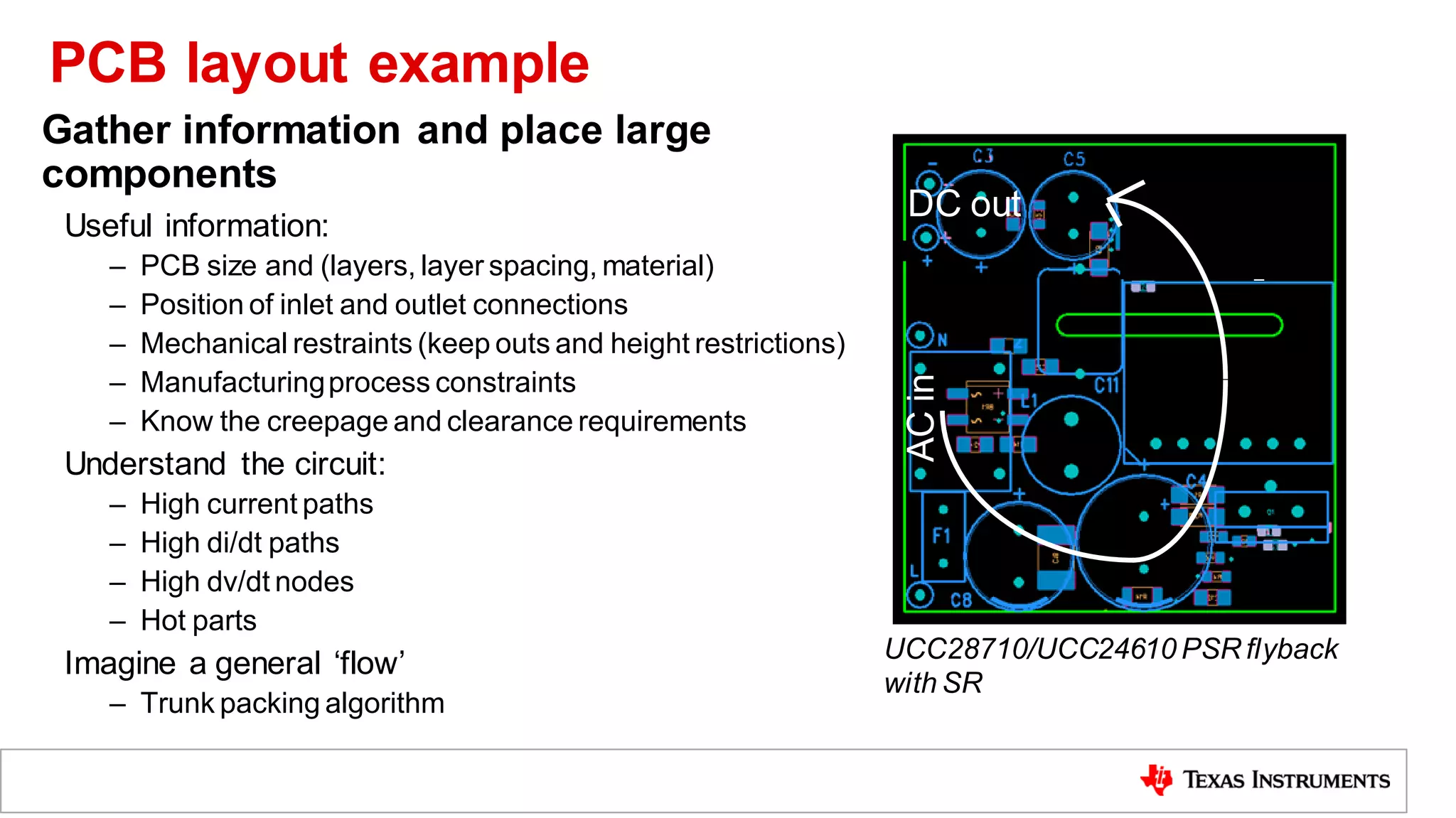
In a switching converter, the "big, heavy suitcases" are the components in the power stage. The "smaller bags" are the sensitive control circuits.
The general order of operations is:
- Place the Power Stage Components: This includes the main switches (FETs), input and output capacitors, and the magnetic components (inductor/transformer). In ZVS converters, this stage also includes the resonant tank components, as they are part of the high-current power path. This entire group is the "noisy" part of the circuit.
- Place the Control and Sensitive Circuitry: This includes the controller IC itself and its supporting cast, like the feedback voltage divider, current sense resistors, and bootstrap capacitors. This is the "quiet" part of the circuit that needs to be protected.
- Place Ancillary Components: Connectors, indicators (LEDs), and other non-critical parts are placed last.
The primary goal of this separation is to keep the noisy power currents from corrupting the sensitive analog signals used by the controller.
2. Strategy for Power and Resonant Component Placement
The placement of the power stage is guided by the principles from our last two lessons: minimize the area of high-current, high-frequency loops.
Let's watch a practical demonstration. While this video uses a standard buck converter, the thought process for placing the power components is universal.
(Sponsored) Switching Regulator PCB Design - Phil's Lab #60
In this video, "(Sponsored) Switching Regulator PCB Design," Phil's Lab provides an excellent step-by-step walkthrough of placing the core power components. Pay close attention to the logic behind each placement decision.
Please watch from 09:38 to 15:09. Observe how the placement proceeds: starting with the controller IC, then the input capacitor, the inductor, and finally the output capacitors, all with the goal of creating tight, direct paths for current.
As the video demonstrates, the process is methodical:
- Start with the Switches: Place the FETs or the switching controller IC near the center of the converter's dedicated area.
- Add Input Capacitors: Place the input bypass capacitors immediately adjacent to the switches to minimize the input "hot loop" area. This is the single most critical placement for controlling EMI.
- Add the Main Magnetic: Place the inductor (for a buck/boost) or transformer (for a flyback/full-bridge) close to the switch node. This keeps the trace with the highest voltage swings () short, which minimizes its ability to radiate noise.
- Add Output Capacitors: Place these close to the output of the magnetic element to complete the output filtering loop.
Placement in ZVS Topologies
In ZVS converters, the resonant tank components (inductors and capacitors) are integral to the power stage and carry high currents. Their placement is just as critical.
Let's examine a layout guide for a full-bridge ZVS wireless power transmitter. This document gives a perfect real-world example of a placement hierarchy.
P9241-G Tx Reference Design Layout Guide
This guide from Renesas, "P9241-G Tx Reference Design Layout Guide," specifies the exact order for placing power components.
Please read sections 3 ("Power Circuits") and 4 ("Bridge Routing"). Pay special attention to the numbered list in section 3 which gives the order of priority for placement. Note that the FETs, input capacitors, and Zero-Voltage Switching (ZVS) Capacitors are all high-priority items placed together.
The key takeaways from the Renesas guide are:
- Co-location: The full-bridge FETs are placed near the resonance components.
- Clear Priority: A clear placement order is defined, ensuring the most critical loops are handled first. The ZVS capacitors, which are essential for controlling the switching transition, are placed right next to the corresponding FETs. This minimizes the inductance in the path that enables ZVS, making the transition fast and efficient.

3. Strategy for Control and Sensitive Circuitry Placement
Once the noisy power stage is laid out, the next step is to place the sensitive control circuitry. The guiding principle here is isolation.
There are two main strategies for isolation:
- Physical Distance: Keep sensitive components and traces physically far from high-noise areas like the switch node and the inductor/transformer.
- Grounding: Use careful grounding techniques to prevent noisy power-stage currents from flowing under the sensitive analog components and corrupting their ground reference.
Key Sensitive Areas and Their Placement Strategy
- The Controller IC: Position the IC so its sensitive analog pins (like feedback and current sense) point away from the power stage, and its high-current gate driver pins point towards the switches.
- Voltage Feedback Network: This is typically a high-impedance voltage divider that senses the output voltage.
- Placement: Place the resistors close to the output capacitors to get an accurate reading of the final DC output. Crucially, route the feedback trace back to the controller IC away from the magnetic field of the inductor and the electric field of the switch node.
(Sponsored) Switching Regulator PCB Design - Phil's Lab #60
Let's return to the Phil's Lab video to see how to handle the feedback trace.
Watch from 22:37 to 23:55. Notice how the feedback trace is intentionally routed away from the inductor to avoid noise coupling. This is a critical detail in any switching converter layout.
- "Quiet" vs. "Noisy" Ground Areas: The ground for the power stage carries large, fast-switching currents. The ground for the analog control circuitry should be a calm, stable reference.
- Placement: A common and highly effective technique is to create a separate "analog ground" or "quiet ground" plane for the controller and its sensitive components. This quiet ground is then connected to the main "power ground" at a single, carefully chosen point. This is known as a star ground connection. It ensures that the noisy power currents don't share a path with the sensitive control signals.
This concept is clearly explained in the layout guidelines for a ZVS flyback converter.
Design guide for ZVS QR flyback converter using CoolSET ...
This design guide for an Infineon ZVS QR flyback converter provides excellent advice on grounding strategy.
Read the bullet points in section 4, "PCB layout considerations." Focus on the recommendation to "Star at the ground of the primary bulk capacitor" and how it separates the signal grounds, power ground, and others. Also, look at the layout example in Figure 13 to see a visual representation of the component grouping.
Test your understanding!
You are reviewing the PCB layout for an Active Clamp Flyback converter. You notice the following:
The main power switch and the flyback transformer are on one side of the board. The controller IC is on the opposite side. The feedback resistors that sense the output voltage are placed right next to the noisy switch node of the main power switch.
Based on the placement strategies we've discussed, identify two major issues with this layout and explain why they are problematic.
Show answer
There are two significant problems with this layout:
-
Poor Placement of Feedback Resistors: Placing the high-impedance feedback resistors next to the switch node is a critical error. The switch node has very high (fast voltage swings) and will capacitively couple noise directly into the sensitive feedback signal. This can make the output voltage regulation unstable. The correct strategy is to place the feedback resistors near the output capacitors and route the feedback trace away from all noise sources.
-
Separation of Controller and Switches: Placing the controller IC far from the power switches it's driving is inefficient and risky. The long gate drive traces required to connect them will have high parasitic inductance. As we learned in the first lesson of this module, this leads to slow switching, ringing on the gate signal, increased losses, and potential for spurious turn-on. The controller's gate driver pins should be as close as possible to the MOSFET gates.
Conclusion
In this lesson, we've built a strategic framework for component placement in ZVS converters. By understanding the hierarchy of placement and the distinct needs of the power and control sections, you can now analyze a PCB layout from a high level and quickly spot good design practices and critical flaws.
Key Takeaways:
- Follow a Hierarchy: Always place the critical, high-power, noisy components first (switches, magnetics, resonant components), then arrange the sensitive, quiet control circuitry around them.
- Cluster the Power Stage: Group all power stage components to create the smallest possible high-current loops, minimizing parasitic inductance and EMI. This includes the ZVS resonant components.
- Isolate the Control Stage: Protect the controller IC and its sensitive analog inputs (feedback, current sense) from noise through physical separation and dedicated "quiet" grounding (star ground).
- Route Sensitive Traces Carefully: Traces like the feedback line must be routed away from noise sources like the switch node and inductor.
In our final lesson for this module, we'll address a common real-world problem. Even with an excellent layout, parasitic elements can cause voltage spikes that exceed component ratings. We will assess the role and implementation of snubber networks, which are circuits added specifically to absorb this energy and protect your components.