Following up on our last lesson where we designed a data selector, this session introduces its logical counterpart. In the previous lesson, you built a Multiplexer (MUX), a crucial component for choosing one data signal from many sources. Today, we'll construct the inverse: a Demultiplexer (DMUX), which takes a single data signal and routes it to one of many possible destinations.
Your learning goal for this lesson is to design a demultiplexer using the basic logic gates you're already familiar with. Mastering the DMUX is essential for your project. While the MUX is used to read data from a specific register onto a shared data bus, the DMUX is used to write data from that bus to a specific register or memory location. Together, they form the core of the data routing system in your computer.
What is a Demultiplexer?
A Demultiplexer, or DMUX, is a combinational circuit that performs the opposite function of a multiplexer. It has a single data input, a set of "select" lines, and multiple output lines. Based on the binary value of the select lines, the circuit connects the data input to exactly one of the output lines. All other output lines will be held at a value of 0.
Think of it as a postal worker distributing mail. The mail (the data input) arrives in a single stream, and the address on the envelope (the select lines) determines which mailbox (the output line) it gets delivered to.
For a formal introduction, the following video from Neso Academy provides a clear definition and explains the key principles.
Introduction to Demultiplexer | 1:2 DEMUX
This video, "Introduction to Demultiplexer," establishes the core concept of a DMUX.
Please watch the first two segments. The first part, "What is a Demultiplexer?", explains its function as a "data distributor" and how it acts as the reverse of a MUX. The second part explains the relationship between the number of output lines (n) and the number of select lines (m), which is n = 2^m.
Designing a 1-to-2 Demultiplexer
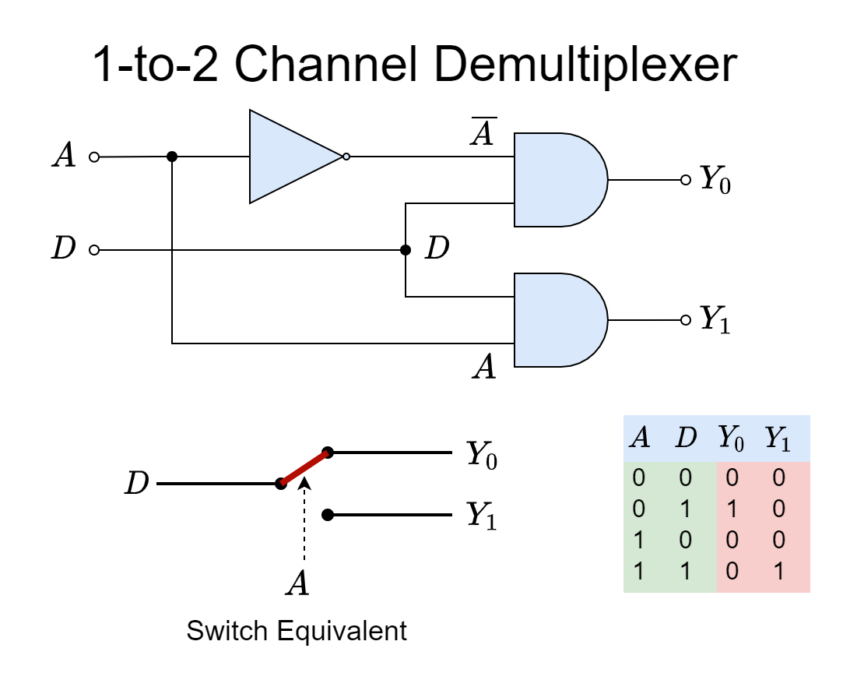
Let's start with the simplest possible DMUX: a 1-to-2 Demultiplexer. This circuit has one data input , one select line , and two outputs, and .
The logic we need to implement is straightforward:
- If select line , the data input should be passed to output , and should be 0.
- If select line , the data input should be passed to output , and should be 0.
Given your background in Boolean math, we can express this logic for each output line:
- is active only when (or ). It should receive the data under this condition. So, the expression is: .
- is active only when . It should receive the data under this condition. The expression is: .
These two equations give us a complete recipe for the circuit. We need one NOT gate to invert the select line into , and two AND gates to produce the final outputs.
The image below shows this exact implementation, along with a truth table and a helpful "switch equivalent" to visualize the concept.
The Nand2Tetris course, which aligns closely with your goal of building a computer from the ground up, uses a hardware description language (HDL) to define these gates. This representation might feel familiar given your experience with C. The logic is identical to our Boolean expressions.
From Nand to Tetris – Victor Penso
This article section from a guide on the Nand2Tetris course provides a pseudo-code description and a concrete implementation of a DMUX.
In the "Project 1" section, please read the pseudo-code for a 2-way demultiplexer. Then, scroll down to the "Solution to Project-1" and examine the HDL code for the DMux chip. Notice how it directly implements our two Boolean equations using NOT and AND gates.
Scaling the Design: The 1-to-4 Demultiplexer
To be useful in a computer, we need to distribute data to more than just two locations. Let's scale our design up to a 1-to-4 Demultiplexer. Following the rule , to control 4 output lines, we will need select lines. Let's call them and .
The two select lines form a 2-bit binary number that acts as an "address" for the output:
- If , data goes to output .
- If , data goes to output .
- If , data goes to output .
- If , data goes to output .
The following video walks through the entire design process for a 1-to-4 DMUX, from the truth table to the final circuit diagram.
The video "1:4 Demultiplexer" from Neso Academy provides a detailed construction of this more complex circuit.
Please watch the following segments: First, observe how the truth table is constructed. Next, see how the Boolean expressions for each of the four outputs are derived from the table. For example, for output Y_2 to be active (S_1S_0=10), the expression becomes Y_2 = D \cdot S_1 \cdot \bar{S_0}. Finally, watch how these expressions are translated into the final logic circuit using AND and NOT gates.
The resulting circuit diagram is a logical extension of our 1-to-2 design. It simply requires more AND gates (one for each output) and more complex input conditions based on the two select lines. The image below shows a clean implementation of this circuit.

This scaling can continue. A 1-to-8 DMUX would require 3 select lines, and a 1-to-16 DMUX would require 4 select lines. This ability to use a binary address to select a specific output channel is exactly what you'll need later to write data to a particular location in memory.
Conclusion
In this lesson, you have designed the Demultiplexer, a fundamental component for directing the flow of information in a computer. You now have both the "selector" (MUX) and the "distributor" (DMUX) in your digital toolkit.
Here are the key takeaways:
- A Demultiplexer (DMUX) is a combinational circuit that routes a single data input to one of outputs, controlled by select lines.
- It is the functional inverse of a Multiplexer.
- The design of a DMUX is derived from its truth table, resulting in a set of Boolean expressions—one for each output line.
- Each expression is typically a simple ANDing of the data input with the corresponding combination of select lines (and their inversions).
- In a computer system, a DMUX is critical for tasks like writing data from a central bus to a specific register or memory address.
You have now built the essential components for routing data. In the next lesson, we will shift our focus from moving data to processing it. You will design a Half Adder, which performs binary addition on two bits. This is the first step toward building the Arithmetic Logic Unit (ALU)—the computational core of your future CPU.