Welcome back! In our last lesson, you successfully designed a Half Adder, the first essential component for performing arithmetic in your future CPU. We saw that it correctly adds two single bits but has a crucial limitation: it cannot accept a "carry-in" bit from a previous calculation. This makes it unsuitable for adding numbers larger than one bit.
Today, we will overcome that limitation by designing a Full Adder. This circuit is the cornerstone of computer arithmetic. You will learn how to define its logic and, most importantly, how to construct it by combining the Half Adders you've already mastered. This lesson is a perfect example of a core engineering principle: building complex systems by composing simpler, reusable components.
The Problem: Adding with a Carry
When adding multi-digit numbers by hand, you add one column at a time. If a column's sum is 10 or more, you write down the units digit and carry the '1' over to the next column. Binary addition is the same. The Half Adder can handle the first column (the least significant bit), but for every subsequent column, we need a circuit that can add three bits: the two input bits for that column (A and B) plus the carry bit from the column before it (Cin).
The following video provides an excellent illustration of why the Half Adder is insufficient for multi-bit addition and why a new component with a carry-in is necessary.
Combinational Devices 1: Half Adder and Full Adder
This segment from the "Down to the Wires" channel demonstrates multi-bit binary addition and highlights the need for a circuit that can handle a carry-in bit.
Watch from the start of this section. Focus on the example of adding 1011 + 1. Notice how at the second bit position, you need to add three numbers: 1 (from 1011), 0 (from the added number, implicitly), and the 1 that was carried over from the first column. This is the problem the Full Adder solves.
Defining the Full Adder
A Full Adder is a combinational circuit that adds three bits and produces two outputs.
- Inputs: A, B, and Cin (Carry-In).
- Outputs: S (Sum) and Cout (Carry-Out).
To design this, we'll follow the same process as before: start with a truth table. This table must now account for all 8 possible combinations of the three inputs.
This article from CircuitVerse provides the formal definition of a Full Adder, including its block diagram and truth table.
Under the main "Full adder" heading, read the Introduction. Then, study the Block diagram and the Truth table. As you examine the truth table, try to verify a few rows yourself. For example, for inputs A=1, B=1, Cin=1, the sum is 1+1+1 = 3, which is 11 in binary. This means the Sum output should be 1 and the Carry-Out should be 1.
The Intuition: Adding Three Bits by Adding Two at a Time
How can we build this using our existing Half Adders? Think about how you'd add three numbers like 5, 8, and 2 in your head. You would likely add the first two (5 + 8 = 13) and then add the third number to that result (13 + 2 = 15).
We can apply this exact same logic to our circuit. To add A, B, and Cin:
- First, use a Half Adder to add A and B. This will give us a preliminary sum (let's call it S1) and a preliminary carry (C1).
- Next, use a second Half Adder to add the preliminary sum (S1) to our third input, Cin. The sum output of this second Half Adder will be our final Sum (S). This operation also produces a second carry bit (C2).
This handles the final Sum perfectly. But what about the final Carry-Out (Cout)? A carry-out should be generated if either the first addition (A+B) produced a carry (C1) or the second addition (S1+Cin) produced a carry (C2). This "either/or" condition points directly to combining C1 and C2 with an OR gate.
So, the complete design is: two Half Adders and one OR gate.
Assembling the Circuit
This modular approach is powerful because it allows us to reason about a more complex circuit using simpler blocks we already understand. The following resources provide a clear visual guide and step-by-step instructions for this construction.
First, let's watch a video that walks through the block-level construction and derives the logic for the final Sum and Carry-Out.
This video from Neso Academy is a focused tutorial on building a Full Adder from Half Adders.
Watch the segment from the beginning. The video first reviews the expressions for Half and Full adders, then masterfully demonstrates how to connect two Half Adder blocks and an OR gate to produce the correct final Sum and Carry-out. Pay close attention to how the carry outputs from the two Half Adders are combined.
Now, let's look at this structure in both a detailed logic gate diagram and a higher-level block diagram.
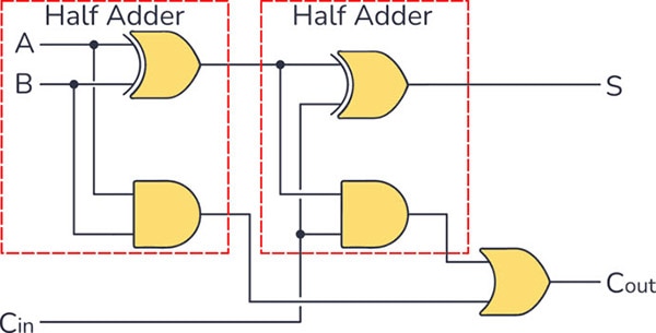

The GeeksforGeeks article provides a fantastic step-by-step guide that is worth reading to solidify your understanding of the wiring.
Implementation of Full Adder Using Half Adders
This article provides detailed, step-by-step instructions for building the Full Adder, first at the logic gate level and then at the block diagram level.
First, read the section "Implementation of Full Adder Using Half Adders". The text walks through the connections shown in the logic gate diagram. Then, read the next part, which starts with the block diagram implementation. This reinforces the concept at a higher level of abstraction, which is key for building even more complex circuits later.
As a final confirmation, the Neso Academy video you watched also contains an algebraic proof showing that the carry logic we derived (C1 OR C2) is mathematically identical to the standard boolean expression for a Full Adder's carry. Since you're familiar with Boolean math, you may find this interesting.
This optional segment provides the algebraic proof for the carry logic.
If you're interested, watch from this timestamp. The instructor proves that (A AND B) OR ((A XOR B) AND Cin) is equivalent to the textbook definition (A AND B) OR (A AND Cin) OR (B AND Cin). This confirms our modular design is logically sound.
Conclusion
In this lesson, you have taken a significant step forward by designing the Full Adder. You've seen how a component's limitations can be overcome by designing a more capable version, and more importantly, how we can build that new version by composing the simpler components we already have.
Here are the key takeaways:
- A Full Adder is a circuit that adds three input bits (A, B, Cin) to produce a Sum and a Carry-Out.
- It solves the critical limitation of the Half Adder, enabling it to be used in any column of a multi-bit addition.
- A Full Adder can be constructed from two Half Adders and one OR gate.
- This modular design approach (building complex components from simpler ones) is fundamental to all computer engineering.
You now have the single most important building block for arithmetic in your CPU. In the next lesson, we will see how to chain these Full Adders together to create a multi-bit ripple-carry adder, a circuit capable of adding 4-bit, 8-bit, or even larger binary numbers.