Welcome back! In the last two lessons, you designed the fundamental building blocks of computer arithmetic: the Half Adder and the Full Adder. You saw how the Full Adder improves upon the Half Adder by accepting a carry-in bit, making it suitable for any position in a multi-bit addition.
Today, we'll put that powerful component to work. We are moving up another level of abstraction to construct a circuit that can add not just single bits, but entire binary numbers. This lesson will show you how to chain multiple Full Adders together to create a 4-bit ripple-carry adder. This is the first component you will build that performs a recognizable mathematical operation on multi-bit data, a significant step toward creating the Arithmetic Logic Unit (ALU) for your computer.
The Logic of Multi-Bit Addition
Think about how you add multi-digit numbers on paper, like 18 + 24. You start from the rightmost column (the least significant digits):
- Add
8 + 4to get12. You write down the2and carry over the1. - Move to the next column. You add
1 + 2plus the1you carried over, getting4. - The final result is
42.
Binary addition works exactly the same way. The carry-out from adding one pair of bits becomes the carry-in for the next pair. A circuit that mimics this process is called a ripple-carry adder because the carry signal "ripples" from one stage to the next.
The video below explains and visualizes how you can "daisy-chain" the Full Adders you built in the previous lesson to create this effect.
Logic Gates and the Ripple Carry Adder
This short clip from Computer Science Lessons demonstrates how Full Adder blocks are connected to form a ripple-carry adder.
Watch from this segment. The key takeaway is seeing how the carry out of one Full Adder is physically wired into the carry in of the next one in the chain.
The Architecture of a 4-Bit Adder
To build a 4-bit adder, which adds two 4-bit numbers (let's call them A and B), we will need four Full Adder circuits. Let's denote the bits of A as and the bits of B as .
Here is the high-level architecture:
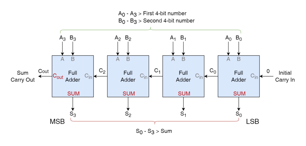
A 4-bit ripple-carry adder built from four Full Adder blocks. The carry-out (Cout) from each stage is connected to the carry-in (Cin) of the next stage, from right to left (LSB to MSB).
Let's break down the connections shown in this diagram:
- Stage 0 (LSB): The first Full Adder on the right adds the least significant bits, and . Its carry-in is tied to
0because there is no preceding calculation. It produces sum bit and a carry-out . - Stage 1: The second Full Adder adds bits and , along with the carry-in from the previous stage, . It produces sum bit and a new carry-out .
- Stage 2: The third Full Adder adds , , and the incoming carry . It produces sum bit and carry-out .
- Stage 3 (MSB): The final Full Adder adds the most significant bits, and , along with the carry . It produces the final sum bit and the overall carry-out of the entire 4-bit addition, .
The final 4-bit sum is represented by the collection of the sum outputs: . The final is also very important; it tells us if the addition resulted in a value too large to be represented by 4 bits (an "overflow").
The following video provides a fantastic, detailed walkthrough of this exact process, showing each connection and explaining the flow of data.
4 Bit Parallel Adder using Full Adders
This Neso Academy video provides a clear, step-by-step construction of a 4-bit parallel adder using Full Adder blocks.
Watch the core construction part from this section. Pay close attention to how the carry output from one block becomes the carry input for the next. Notice how the final 5-bit result is composed of the four sum bits (S0-S3) and the final carry bit (C3).
Building the Circuit
Now that you understand the architecture, let's dive into the details of building it. The following article provides a concise guide and also introduces a critical real-world concept: propagation delay.
Mastering Binary Addition: Building a 4-Bit Ripple Carry Adder
This DigiSim.io blog post explains the architecture of the ripple-carry adder and gives practical steps for building it in a simulator.
First, read the section "What is a Ripple Carry Adder?" for a clear definition. Next, read "The Architecture of the Chain", which details the four stages of the 4-bit adder. Finally, read the section "Building the Circuit". Although it refers to a specific simulator, the steps are universal and describe exactly how you would connect your Full Adder components in any simulation environment.
The design's modularity is its main strength. You can see this clearly in hardware description languages (HDLs), which are used to design real chips. The following article shows HDL code for a 16-bit adder. You don't need to understand the syntax, but look at the PARTS section to see the beautiful, repetitive pattern of chaining Full Adders.
Building own Computer with Nand2Tetris: Project II
This blog post shows an implementation of a 16-bit adder, which is a great example of the scalability of the ripple-carry design.
Scroll down to the heading "16-bit Adder" and look at the code block. Notice how it's just a long list of FullAdder components, where the carry from one line (carr0) becomes the input c on the next line (c=carr0). This is the software equivalent of the block diagrams we've been studying. Note: The code uses a HalfAdder for the first stage. This is a valid optimization if the initial carry-in is always 0. However, using a FullAdder with its carry-in tied to 0, as we've discussed, creates a more uniform and repeatable structure, which is often preferred in hardware design.
Here is what a 4-bit ripple-carry adder looks like when you zoom in and see all the individual logic gates you've learned about. This is the culmination of everything you've done so far in this module.
A complete circuit diagram of a 4-bit ripple-carry adder. Each block of gates represents one of the Full Adders from our block diagram, all wired together to add two 4-bit numbers.
A Look Ahead: The Problem with Rippling
The DigiSim.io article you read mentioned a key drawback: propagation delay. The final stage (the MSB) cannot produce a correct sum until the carry from the first stage has "rippled" all the way through the chain. For a 4-bit adder, this is quick. But for a 64-bit adder in a modern CPU, this delay would be far too long.
This physical limitation is a core challenge in CPU design. While the ripple-carry adder is logically correct, faster (and more complex) designs like the Carry-Lookahead Adder were invented to solve this problem. We won't build one in this course, but it's important to understand that every design choice has trade-offs, in this case, simplicity versus speed.
Conclusion
You have now successfully designed a circuit capable of multi-bit arithmetic. By chaining together the Full Adders you mastered in the previous lesson, you've created a functional 4-bit ripple-carry adder.
Here are the key takeaways from this lesson:
- A multi-bit adder can be constructed by chaining together multiple Full Adder blocks.
- In a ripple-carry adder, the carry-out from each stage is fed as the carry-in to the subsequent stage.
- The first stage (LSB) has its carry-in set to
0. The final carry-out from the last stage (MSB) indicates an unsigned overflow. - This design is simple and modular, but its speed is limited by the propagation delay of the carry signal as it "ripples" through the chain.
You now have the "addition" part of your future Arithmetic Logic Unit. In the next lesson, we will build the "logic" part—a unit for performing bitwise operations like AND and NOT on multi-bit numbers.