Welcome to the next step in building your computer's memory. In the previous lesson, you mastered the D Flip-Flop, a reliable, synchronized component that can store a single bit of information. You saw how it uses a clock signal to update its state at a precise moment, solving the problems of asynchronous latches.
However, a D Flip-Flop on its own has a limitation: it captures a new value on every single rising clock edge. For our computer, we need more control. We need a component that can not only store a bit but also decide when to change it and when to hold its current value, even as the clock continues to tick.
In this lesson, you will build that component: a 1-bit register. By combining the D Flip-Flop you just learned about with a Multiplexer from a previous module, you will create a memory cell with a load control. This fundamental circuit is the building block you'll replicate to create your CPU's registers and, eventually, your computer's main memory (RAM).
The Need for Controlled Loading
Imagine a busy highway—your computer's data bus—with data constantly changing. A plain D Flip-Flop connected to this bus would be like a driver erratically swerving into a lane on every green light. It would grab whatever data happens to be on the bus at every clock tick, whether you want it to or not.
This isn't practical. We need to be able to tell our memory cell: "Hold on to the value you have now. Ignore the bus." and then, at a specific moment: "Okay, now load the value from the bus." This requires a control mechanism.
Introduction to Registers | What is Shift Register? Types of Shift Registers
The video "Introduction to Registers" explains this exact problem. It highlights why a simple group of flip-flops isn't sufficient for a practical computer system.
Watch the segment from this timestamp. The presenter discusses why a register that loads data on every clock transition is impractical and how it would monopolize the data bus, leading to the need for a control system.
The Logic of a Register
To solve this, we introduce a new control input, which we'll call load. The behavior we want to implement is simple and can be expressed with a conditional statement. For any given point in time t, the output at the next clock tick, out(t+1), is determined as follows:
- If
loadis 1, the register should update:out(t+1)becomes the value of theinsignal at timet. - If
loadis 0, the register should hold its value:out(t+1)remains the same as the current output,out(t).
This logic is the formal definition of a 1-bit register.
From Nand to Tetris – Victor Penso
The course materials for Nand to Tetris, a project very similar to your goal, provide a concise definition for this component, which they call a "Bit" chip.
In the "Unit 3" section, find the subsection on Flip-Flops. Read the short definition of a 1-bit register and study the simple if/else logic that describes its behavior.
This if/else logic should be familiar. It's the exact function performed by a Multiplexer (MUX), a component you've already built. This makes the implementation surprisingly elegant.
The Solution: A Multiplexer-Controlled Feedback Loop
We can implement the register's logic by feeding the D Flip-Flop's input from a 2-to-1 MUX. The load signal will act as the MUX's selector.
Here is the setup:
- MUX Input 'A' (selected when
load=0): The D Flip-Flop's current output,Q. - MUX Input 'B' (selected when
load=1): The new data from an externalinpin. - MUX Output: This goes directly into the D Flip-Flop's data input,
D.
When load is 0, the MUX selects its 'A' input. This creates a feedback loop: the flip-flop's own output is fed back into its input. On the next clock tick, it simply re-loads the value it already has, effectively holding its state.
When load is 1, the MUX selects the 'B' input, passing the new external data to the flip-flop. On the next clock tick, this new value is captured.
[PDF] ECE 120: Introduction to Computing A Register Stores a Set of Bits ...
This slide deck from an introductory computer engineering course provides a clear, visual explanation for using a MUX to implement the load functionality.
Start on slide 6, titled "LOAD Controls Whether a Register Loads a New Value", which directly proposes this solution. Then, carefully study the diagram on slide 7, "A 1-Bit Register with a LOAD Input". This schematic is the blueprint for our 1-bit register.
Here is what the final circuit looks like in a simulator like Logisim.

Under the Hood: The Gate Logic
While we can think of the MUX as a single component, it's helpful to remember that it's built from basic logic gates. The MUX in our register circuit is just a neat abstraction for a specific arrangement of AND, OR, and NOT gates.
Designing and building a 1-bit register - 8 bit register - Part 3
In his video "Designing and building a 1-bit register," Ben Eater explains exactly how this control logic works at the gate level. He doesn't use a MUX component, but instead builds the equivalent logic from scratch.
Watch from this segment. Follow his diagram and trace the flow of 0s and 1s for both cases: when the load input is low (holding the value) and when the load input is high (loading a new value). You'll see how the AND and OR gates effectively "select" which data reaches the D Flip-Flop.
Tracing a Register's Behavior
To solidify your understanding, let's trace the state of a 1-bit register over time using a timing diagram.
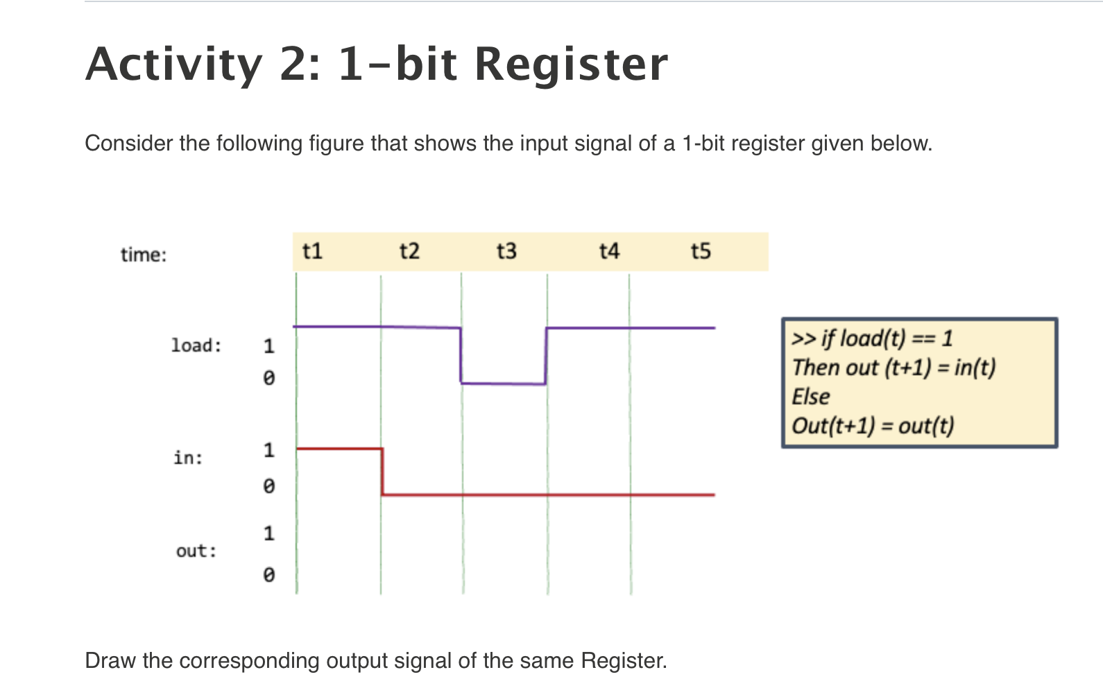
Let's walk through the first couple of steps together. Assume the output out starts at 0 before time t1.
- At
t1: Theloadsignal is 1 and theinsignal is 1. The rule saysout(t+1) = in(t). Therefore, at the next clock tick (t2), the output will become 1. - At
t2:loadis still 1, butinhas dropped to 0. The ruleout(t+1) = in(t)is still active. So, at the next clock tick (t3), the output will be updated to match the input, becoming 0. - At
t3:loaddrops to 0. The rule now becomesout(t+1) = out(t). The register will now hold its current value. Sinceoutis currently 0, it will remain 0 at timet4.
Now, try to determine the value of out at time t5 and beyond. This exercise is key to understanding how sequential circuits behave over time.
Conclusion
You have now designed a 1-bit register, a memory cell that gives you precise control over when to store data. This is a huge leap from the simple flip-flop, moving us from a passive memory element to an active, controllable component.
Key Takeaways:
- A register is a memory circuit that can be instructed to either load new data or hold its current value.
- This control is achieved by adding a
loadsignal. - The logic for a 1-bit register is
if (load) out = in, else out = out. - This
if/elselogic is implemented perfectly by a 2-to-1 Multiplexer, which selects between the new input and the current, fed-back output. - The combination of a D Flip-Flop for storage and a MUX for control forms the fundamental building block of computer memory.
In the next lesson, we will scale this design up. You will take the 1-bit register you've just created and combine several of them to construct an n-bit register, capable of storing a multi-bit value like a character or a number. This will be the first component you build that directly corresponds to the registers in a real CPU.