In our last session, you successfully built a 1-bit register, a fundamental memory cell that can hold its state or load a new one on command. This gave you precise control over a single bit of data. Now, we're going to scale up that concept to build something much more powerful and directly applicable to a real computer: a component that can store an entire "word" of data.
This lesson bridges the gap between storing a single 'on/off' state and storing meaningful information like numbers or characters. You will learn how to construct an n-bit register by combining the 1-bit registers you've already mastered. This is a critical step, as these n-bit registers will form the core of your CPU's internal memory and prepare us for building the computer's main Random Access Memory (RAM).
From Bits to Words
So far, we have worked with individual bits. However, a computer rarely operates on just one bit at a time. It processes groups of bits called words. The number of bits in a word, known as the word size, is a fundamental characteristic of a computer's architecture. Common word sizes are 8-bit, 16-bit, 32-bit, or 64-bit. For example, in C, a char variable is typically stored as an 8-bit word.
To store a word, we need a device that can hold multiple bits simultaneously. This device is the n-bit register.
[PDF] Registers and Counters - KFUPM
This document provides a concise introduction to the concept of an n-bit register. It formally defines what a register is and illustrates the logic for adding a load control.
Read the first few slides to understand the basic definition and structure. Start with slide 3, "Register", which shows a 4-bit register made of four D Flip-Flops. Then, read slide 4, "Register Load (or Enable)", which raises the key design question. Finally, study the solution on slide 5, "Register with Parallel Load", which shows the complete, general design for an n-bit register with load control.
The core idea is beautifully simple and demonstrates a key principle in digital design: modularity. To build a register that can store n bits, we simply take n of our 1-bit registers and arrange them side-by-side.
Assembling the N-Bit Register
Let's visualize how to connect these 1-bit modules to create a larger, unified component. Imagine we want to build a 4-bit register. We will need:
- Four instances of our 1-bit register (the D-Flip-Flop + MUX circuit from the last lesson).
- A 4-bit input bus, which we'll call
in[3..0]. Each wire of this bus (in[0],in[1],in[2],in[3]) carries one bit of the word we want to store. - A 4-bit output bus,
out[3..0], to read the stored word.
The wiring is straightforward:
- The input
in[0]connects to the data input of the first 1-bit register. in[1]connects to the second register, and so on.- The
outfrom each 1-bit register connects to the corresponding wire of the output bus.
The crucial part is how we handle the control signals. For the register to act as a single, cohesive unit, the clock and load inputs must be shared. A single clock line is fanned out to the clk input of all the 1-bit registers. Similarly, a single load line connects to the load input of all of them.
This ensures that when the load signal is asserted, all bits of the new word are loaded from the input bus simultaneously on the next rising clock edge. When load is de-asserted, all bits hold their value in unison.
[PDF] CprE 281: Digital Logic - Iowa State University
These slides from Iowa State University provide excellent, clear diagrams showing exactly how to scale from a 1-bit register to a multi-bit register.
Focus on the diagrams showing the "Parallel-Access Register". Start with the 2-bit example, then look at the 3-bit and 4-bit versions. Pay close attention to how the Clock and Load lines are wired to all the flip-flop/MUX units, while the data lines (In_0, In_1, etc.) are kept separate.
Visualizing the Complete Circuit
When these individual bit-slices are combined, you get a larger, more complex circuit. However, it's just a repetition of the same simple pattern. The image below shows what a 16-bit register looks like in a logic simulator.

This circuit perfectly embodies the learning outcome. You can see the 16 parallel rows, each one a 1-bit register. The load signal at the top left and the clk signal are distributed to every single row, ensuring synchronized operation.
Abstraction and Integrated Circuits
As you can see, even a 16-bit register becomes visually complex. To build a full computer, we can't work at this level of detail for every component. The next step is abstraction. Once we have designed and tested our n-bit register, we can encapsulate it in a single "black box" in our diagrams. We only need to care about its inputs (in[n-1..0], load, clk) and its output (out[n-1..0]).
This is exactly what happens in real-world hardware design. Engineers don't build registers from individual gates every time. They use integrated circuits (ICs) that contain one or more pre-built registers.
Designing and building a 1-bit register - 8 bit register - Part 3
In his video series on building an 8-bit computer, Ben Eater faces this exact decision: build from basic gates or use a pre-made register chip.
Watch the segment from this timestamp. He discusses the trade-off and introduces the 74LS173, a 4-bit register IC. Looking at the logic diagram inside this chip, you'll see it's almost identical to the MUX-based design you've learned. This is a great example of how our theoretical design maps to a physical component.
A Quick Note on Other Register Types
The register we have designed is a parallel-load register, meaning all n bits are loaded at once. This is the most common type used for CPU registers. For context, it's useful to know that other types exist, most notably shift registers. Instead of loading all bits at once, a shift register moves bits in or out one position at a time on each clock cycle, like a bucket brigade.
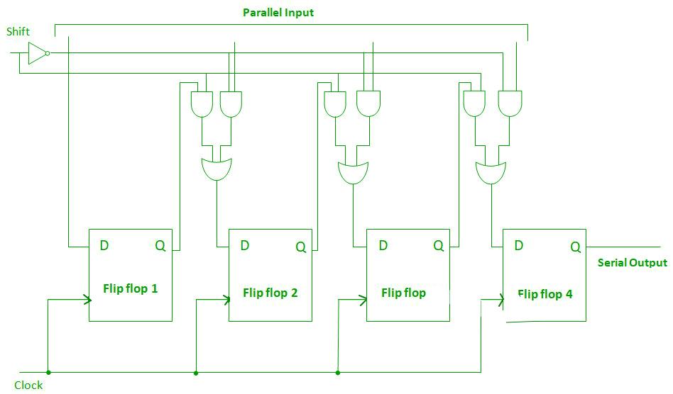
While interesting, shift registers serve a different purpose. For our goal of building a CPU and memory, the parallel-load register is the component we need.
Conclusion
You have now scaled your single-bit memory cell into a multi-bit register capable of storing a full word of data. This is a cornerstone of computer architecture, moving us from the world of pure logic into the realm of data processing and storage.
Key Takeaways:
- An n-bit register is built by combining n 1-bit registers in parallel.
- Data is transferred to and from the register using n-bit wide buses.
- The
clockandloadsignals are shared across all bit-slices to ensure synchronized operation, so the register acts as a single unit. - This modular design can be abstracted into a single component, which is essential for managing the complexity of designing a computer.
In the next lesson, you will take this principle of aggregation one step further. We will move from building a single register to constructing a large bank of registers to form the computer's main memory, or Random Access Memory (RAM). To do this, you will first need to design a circuit that can select one specific register out of many: an address decoder.