Hello! In our last lesson, you built your first memory circuit, the SR Latch. You saw how feedback allows a circuit to hold a state, but also discovered its limitations: the unpredictable "invalid state" and its asynchronous nature, where outputs change immediately with inputs.
This lesson takes the crucial next step. We will transform the asynchronous latch into a synchronous, predictable, and robust one-bit memory cell: the Data Flip-Flop, or D Flip-Flop. This is one of the most important building blocks in your computer. By constructing it from the gates you already know, you will create a device that captures a bit of data (D) precisely on the "tick" of a clock signal. This solves the problems of the SR latch and gives us the reliable component we need to start building registers and memory.
From SR Latch to Gated D Latch
Let's first address the SR Latch's "invalid state" problem. Recall that with a NOR-based latch, having both S=1 and R=1 was forbidden. With a NAND-based latch, S'=0 and R'=0 was forbidden. We can eliminate this possibility entirely with a simple trick. If we ensure that the Set and Reset inputs are always opposites, they can never be simultaneously active.
We can enforce this by using a single data input, which we'll call 'D', and an inverter.
- The 'Set' input receives the D signal directly.
- The 'Reset' input receives the inverted D signal (D').
Now, if D=1, we are Setting the latch. If D=0, D' is 1, and we are Resetting the latch. We have effectively created a latch that takes the value on the D input and stores it.
This forms the basis of a Gated D Latch. It combines this D-input logic with the enable-gated SR Latch you may have seen. It has two inputs: D (Data) and E (Enable, which we'll soon call Clock).
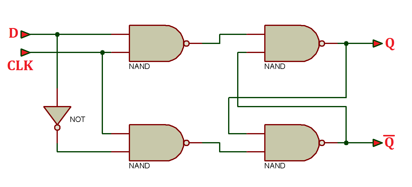
This circuit behaves as follows:
- When the Enable input is HIGH (1), the latch is "transparent." The output Q simply follows the input D. If D changes, Q changes immediately.
- When the Enable input goes LOW (0), the latch "closes." It stores the last value D had and holds it, ignoring any further changes to the D input.
4-bit counter using D-Type flip-flop circuits - 101 Computing
This article from 101 Computing provides a good introduction to this circuit, which it calls a D-Type Flip-Flop. We will make a finer distinction between this and a true flip-flop shortly.
Read the section titled "D-Type Flip-Flop Circuits?". Pay attention to the description of the inputs and outputs. Then, study the truth table and the explanation below it that describes the behavior when the enabler is high versus low.
This Gated D Latch is a useful circuit, but its "transparency" when the clock is high can be a problem in complex systems. We want all our memory elements to update at the exact same instant, not over a period of time. This leads us to the concept of edge-triggering.
The Need for Edge-Triggering
Instead of changing state whenever the clock signal is at a certain level (high or low), a true flip-flop changes state only on a clock edge—the instantaneous moment the clock transitions from low-to-high (a rising edge) or high-to-low (a falling edge).
Ben Eater's video on the D flip-flop provides an excellent visualization of this exact problem. He starts with the level-sensitive D Latch and explains why an edge-triggered device is often more useful.
Watch the first part of the video, where he recaps the D latch and its behavior using a timing diagram. This shows how Q follows D whenever the enable signal is high. Next, watch the crucial explanation of how a flip-flop should behave. He uses a timing diagram to show that the output should only update at the rising edge of the clock, ignoring any changes to D at other times.
As you saw, the desired output is very different. The flip-flop samples the D input at one precise moment and holds that value for the rest of the clock cycle. This discipline is the key to building large, synchronized digital systems. So, how do we build a circuit with this edge-triggered property?
Constructing an Edge-Triggered D Flip-Flop: The Master-Slave Design
The classic method to create an edge-triggered flip-flop is the master-slave configuration. The name describes the architecture perfectly: it consists of two latches connected in series.
- The Master latch is connected to the main D input.
- The Slave latch takes its input from the Master's output and provides the final Q output.
The clock signal controls both, but with a crucial twist: one is enabled by the clock signal, and the other is enabled by the inverted clock signal. This creates a two-stage process.
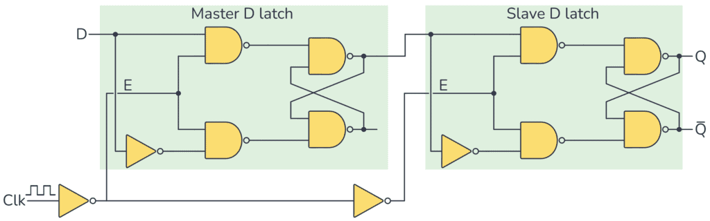
Let's trace how this circuit achieves a positive-edge-trigger (updating when the clock goes from 0 to 1):
-
When Clock is LOW (0):
- The Master latch's enable is HIGH (due to the inverter). It is transparent and continuously samples the external D input.
- The Slave latch's enable is LOW. It is latched, holding the previous value and ignoring the Master's output. The final output Q is stable.
-
When Clock transitions from LOW to HIGH (the rising edge):
- The Master latch's enable flips to LOW. It latches, capturing the exact value of D at the moment of the clock's rise.
- The Slave latch's enable flips to HIGH. It becomes transparent, immediately passing the newly captured value from the Master to the final output Q.
-
When Clock is HIGH (1):
- The Master latch is latched and ignores any changes on the external D input.
- The Slave latch remains transparent, but its input (from the Master) is stable, so the final output Q is also stable.
This clever arrangement ensures the final output Q only ever changes on the rising edge of the clock.
Designing Flip-Flops and Memory Circuits in BOOLR
This article from BOOLR gives a concise, high-level explanation of this exact concept.
First, read the section Synchronizing Data with Clocked D Flip-Flops. This text explains the master-slave principle in words. Then, jump down to the FAQ at the end and read the answer to the question: "What is the difference between a latch and a flip-flop?" This will solidify your understanding of this crucial distinction.
Gate-Level Signal Tracing
Now that you understand the master-slave architecture, let's trace the 0s and 1s through a complete gate-level implementation to see it in action.
Working of Edge-Triggered D Flip Flop
The "EE-Vibes" channel has a very detailed, step-by-step walkthrough of a positive-edge-triggered D flip-flop built from SR latches and NAND gates. While the presenter's pace is deliberate, the detail is perfect for understanding the signal flow.
This video walks through three key scenarios. Follow the presenter's logic in each part: Clock is Low: Watch from this segment to see why the circuit is in a "retaining state." No matter how D changes, the outputs of the first stage (S and R) are held at 1, so the final latch holds its previous value. Clock Rising Edge (D=0): Now watch from this point. The presenter simulates the clock going from 0 to 1 while D is 0. Trace how this change propagates through the gates to make the final output Q become 0. Clock is High: Finally, watch from this segment. The clock is now held high, and the D input is changed from 0 to 1. Observe how the internal feedback loop prevents this change from reaching the output, proving it's not level-sensitive.
This detailed analysis shows that the circuit's output is only vulnerable to change in the brief moment the clock transitions, fulfilling our requirement for a true edge-triggered flip-flop.
Conclusion
You have successfully constructed a D Flip-Flop, the synchronous and reliable workhorse of digital memory. This is a significant step up from the basic SR Latch.
Key Takeaways:
- Latch vs. Flip-Flop: A latch is level-sensitive (transparent when enabled), while a flip-flop is edge-triggered (updates only on a clock transition).
- D Flip-Flop Function: It captures the value of the D input on a single clock edge and holds that value until the next corresponding edge.
- No Invalid State: By design, the D Flip-Flop eliminates the ambiguous or forbidden input combinations that plagued the SR Latch.
- Master-Slave Architecture: A common way to build an edge-triggered flip-flop is by connecting two latches in series (a master and a slave) with inverted clock signals, creating a two-phase capture-and-release mechanism.
You now have a reliable, synchronized, one-bit memory cell. In the next lesson, we will put it to immediate use. You'll take this D Flip-Flop and add a simple control mechanism to create a 1-bit register, the fundamental component you will replicate to build your computer's register file and main memory.