Welcome back! In our last lesson, we established the critical role of the clock signal as the "heartbeat" of a computer, synchronizing all operations. We saw that while combinational circuits like your ALU are essential for computation, they have no memory. They react to inputs, but they can't store results or maintain a state over time.
This lesson introduces the first and most fundamental building block of computer memory: the SR Latch. This simple circuit is the first piece of sequential logic you'll build. Its magic lies in its ability to "remember" a single bit of information (a 0 or a 1) even after the input that set it has been removed. By describing the operation of this basic latch, you will take the first concrete step towards creating stateful components, which are the foundation for registers, RAM, and ultimately, the entire CPU.
The Idea of Latching: Feedback
The key to memory in digital logic is feedback, where a gate's output is connected back to one of its own inputs. This creates a self-reinforcing loop. Let's start with a very simple, intuitive example of this principle.
Ben Eater's video on the SR Latch begins with a brilliant demonstration. He builds a circuit using just a single OR gate with its output fed back into one of its inputs. Watch this first segment to build an intuition for how feedback can "latch" a state.
Watch from the beginning until the end of the OR gate demonstration. Pay close attention to how a momentary press of the button causes the output LED to turn on and stay on. This is the core concept of a latch.
As you saw, this simple circuit can remember that its input was once '1'. However, it has a major limitation: there's no way to turn it off other than cutting the power. To build a useful memory cell, we need the ability to not only set it to '1' but also to reset it back to '0'. This brings us to the SR Latch.
The NOR-based SR Latch
The standard SR Latch is built by cross-coupling two logic gates. Let's examine the version made from two NOR gates. The 'S' stands for Set (which forces the output to 1) and 'R' stands for Reset (which forces the output to 0).
The circuit has two inputs, S and R, and two outputs, Q and Q' (pronounced "Q-not" or "Q-bar"). In a stable state, Q' is always the inverse of Q. Q is considered the primary output of our memory cell.
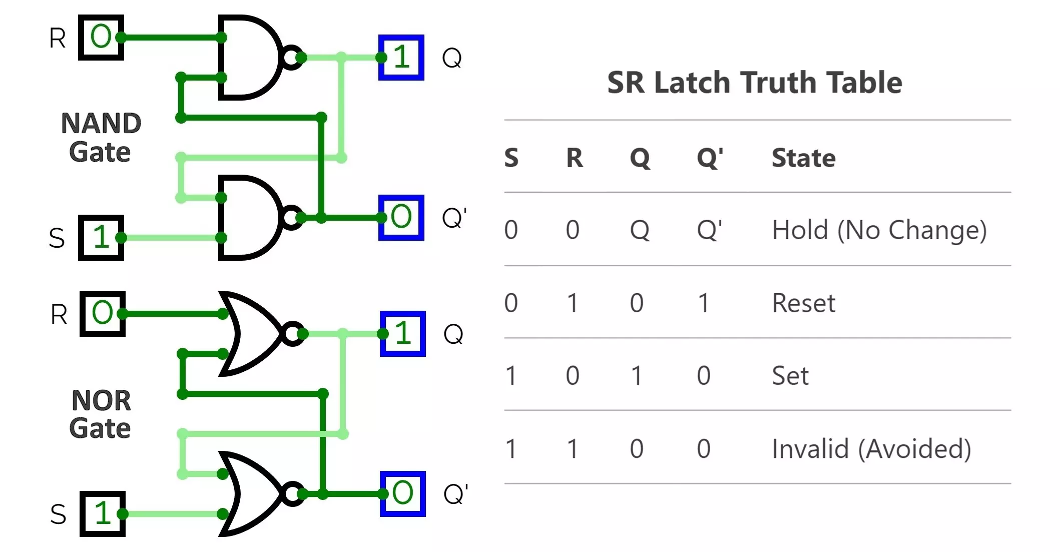
Ben Eater now builds this exact circuit on a breadboard. Following his step-by-step process is the best way to understand how the signals flow and interact.
Continue with the same Ben Eater video. He will now construct and demonstrate the full NOR-based SR latch.
First, watch the segment where he builds and tests the two-NOR-gate circuit. He walks through exactly what happens when you press the 'Set' and 'Reset' buttons, flipping the latch between its two stable states. Then, watch his explanation of the standard terminology (S, R, Q, Q') and the problematic "invalid state" that occurs when you press both buttons at once.
Let's formalize the behavior you just observed.
Analyzing the SR Latch's Operation
The SR Latch has four possible input combinations. Understanding each one is key.
Latches and Flip-Flops 1 - The SR Latch
The "Computer Science Lessons" channel provides a very clear, animated walkthrough of the NOR latch's operation. This will reinforce what you saw in the hands-on demonstration.
Watch the introduction to the NOR gate latch to see the circuit diagram and inputs/outputs defined. Then, carefully follow the step-by-step animation from the demonstration of the set, reset, and hold operations. It visually traces how a change in one gate propagates to the other and stabilizes the circuit.
Here is a summary of the states:
- Hold State (S=0, R=0): This is the memory state. When both inputs are 0, the cross-coupled feedback loop keeps the outputs stable. If Q was 1, it stays 1. If it was 0, it stays 0. The latch is "remembering" its previous state.
- Set State (S=1, R=0): When the S input goes to 1, it forces the output of its NOR gate to 0 (since anything NOR 1 is 0). This 0 is fed to the other NOR gate. With both inputs now 0, its output becomes 1. So, Q becomes 1. The latch is now "set".
- Reset State (S=0, R=1): This is the mirror image of the Set state. The R input going to 1 forces Q to 0. The latch is now "reset".
- Invalid State (S=1, R=1): This state is forbidden. Setting both S and R to 1 tells the latch to simultaneously set and reset. This forces both Q and Q' to 0, which violates the fundamental rule that they must be opposites.
The bigger problem with the invalid state arises when the inputs go from S=1, R=1 back to S=0, R=0. This creates a race condition, where the final state of the latch depends on which of the two gates reacts faster—an unpredictable outcome based on tiny physical variations.
Latches and Flip-Flops 1 - The SR Latch
To fully grasp the problem, watch this segment from the same video, which explains the invalid state and the resulting race condition.
Watch the explanation starting from the invalid circumstance.
The "Chicken and Egg" Problem: Power-On State
A common point of confusion is how the latch behaves when it's first powered on, before any inputs are applied. Both S and R are 0, so which state does it choose?
digital logic - How to understand the SR Latch - Electrical Engineering Stack Exchange
This discussion on Stack Exchange directly addresses this question. It clarifies the difference between what a simulator shows and what happens in a real physical circuit.
First, read the initial question and the top-voted answer's introduction, up to the point where Logisim is mentioned. This frames the problem: the initial state. Next, scroll down to the answer by user "bit-twiddler" and read the second paragraph. This explains why the circuit settles randomly in the real world due to physical race conditions. Finally, read the short answer by "Joe Hass". It makes the crucial point about how to resolve this uncertainty: applying an input will always force the latch into a known, predictable state.
In summary, a latch powers up into a random state. In any real computer system, a "power-on reset" circuit will briefly pulse the reset line of all memory elements to ensure the entire system starts in a known, predictable state (usually all zeros).
The NAND-based SR Latch (Active-Low)
You can also build an SR Latch using two cross-coupled NAND gates. Since you've learned that NAND is a universal gate, it's no surprise it can be used here. The structure is identical, but its behavior is inverted. This is known as an active-low latch.
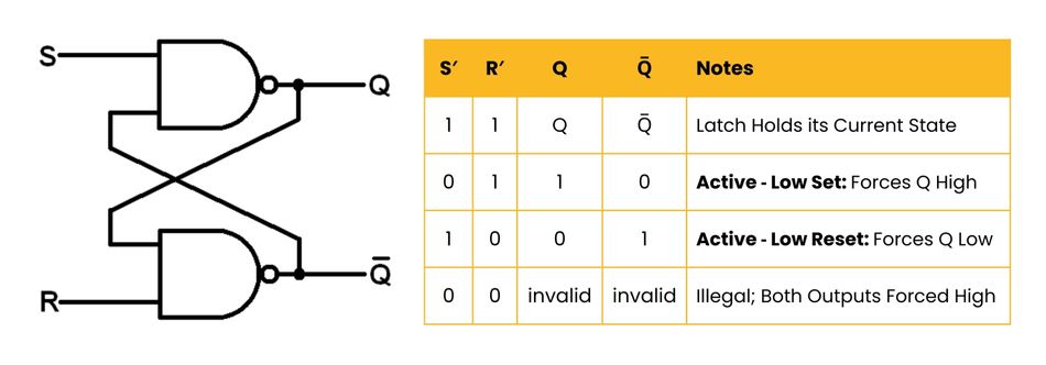
In this configuration:
- The resting or hold state is when S' and R' are both 1.
- To set the latch (make Q=1), you momentarily bring S' to 0.
- To reset the latch (make Q=0), you momentarily bring R' to 0.
- The invalid state occurs when both S' and R' are 0. This forces both Q and Q' to 1.
Understanding the SR Latch: Theory, Design, Truth Tables ...
This section from the Wevolver article provides a concise explanation of the NAND-based latch.
Read the section titled "The SR Latch Constructed from NAND Gates". Focus on the explanation of active-low inputs and study the accompanying truth table to see how it differs from the NOR version.
The choice between a NOR (active-high) or NAND (active-low) latch often comes down to the specifics of the surrounding logic and which type of gate is more readily available in a given technology family.
Conclusion
You have now analyzed the SR Latch, the simplest form of sequential, state-holding logic. This is a significant milestone: you have constructed a circuit that can remember one bit of information.
Key Takeaways:
- Bistability: An SR Latch is a bistable circuit, meaning it has two stable states (Set and Reset) that it can hold indefinitely as long as it has power.
- Feedback: State is held using a positive feedback loop created by cross-coupling two gates (NOR or NAND).
- Operation: The latch has three main modes of operation: Set (store a 1), Reset (store a 0), and Hold (maintain the current value).
- Implementations:
- A NOR-based latch is active-high: a '1' on S or R triggers the action. The invalid state is S=1, R=1.
- A NAND-based latch is active-low: a '0' on S' or R' triggers the action. The invalid state is S'=0, R'=0.
- Asynchronous Nature: The SR Latch is an asynchronous circuit. Its output changes immediately in response to input changes.
This last point is critical. While useful, the asynchronous nature of the SR Latch can be problematic in a large system. We need a way to ensure that our memory elements only change their state in lockstep with the master clock signal. In the next lesson, we will build upon the SR Latch to create a D-type Flip-Flop, a synchronous device that only updates its state on the edge of a clock pulse, bringing us one step closer to building reliable computer memory.