In the previous lesson, you successfully moved from the analog world of transistors to the digital world by building a NAND gate. This was a significant step, as you now have a component that performs a reliable, predictable logical operation.
Today, we will explore the profound power of this single gate. You will learn why the NAND gate is known as a "universal gate." The goal is to implement NOT, AND, and OR gates using only NAND gates to demonstrate this universality. This principle is fundamental to computer design; it means that with a vast supply of just one type of gate, you can construct any digital logic circuit imaginable, including the entire CPU you aim to build.
The Power of Universality
Why is having a "universal gate" so important? In hardware manufacturing, simplicity and repetition are key to efficiency and cost-effectiveness. Instead of needing separate manufacturing processes for AND, OR, and NOT gates, chip designers can perfect the process for creating a single type of gate—the NAND gate—and then wire them together in different patterns to achieve any desired logic. This is the hardware equivalent of building a complex program from a small set of primitive functions.
The following resource provides a concise explanation of what makes a gate universal.
Logic NAND Gate Tutorial with NAND Gate Truth Table
This tutorial from Electronics-Tutorials.ws clearly explains the concept of universality after introducing the NAND gate itself.
Please read the short section titled The "Universal" NAND Gate. It defines the term and states that the three basic gate types can be formed from NAND gates.
Building the Basic Gates from NAND Gates
Now, let's get to the practical implementation. We will build each of the three basic gates—NOT, AND, and OR—using nothing but the NAND gate you studied in the last lesson.
The image below shows the circuit diagrams for these constructions. We will analyze each one in turn.
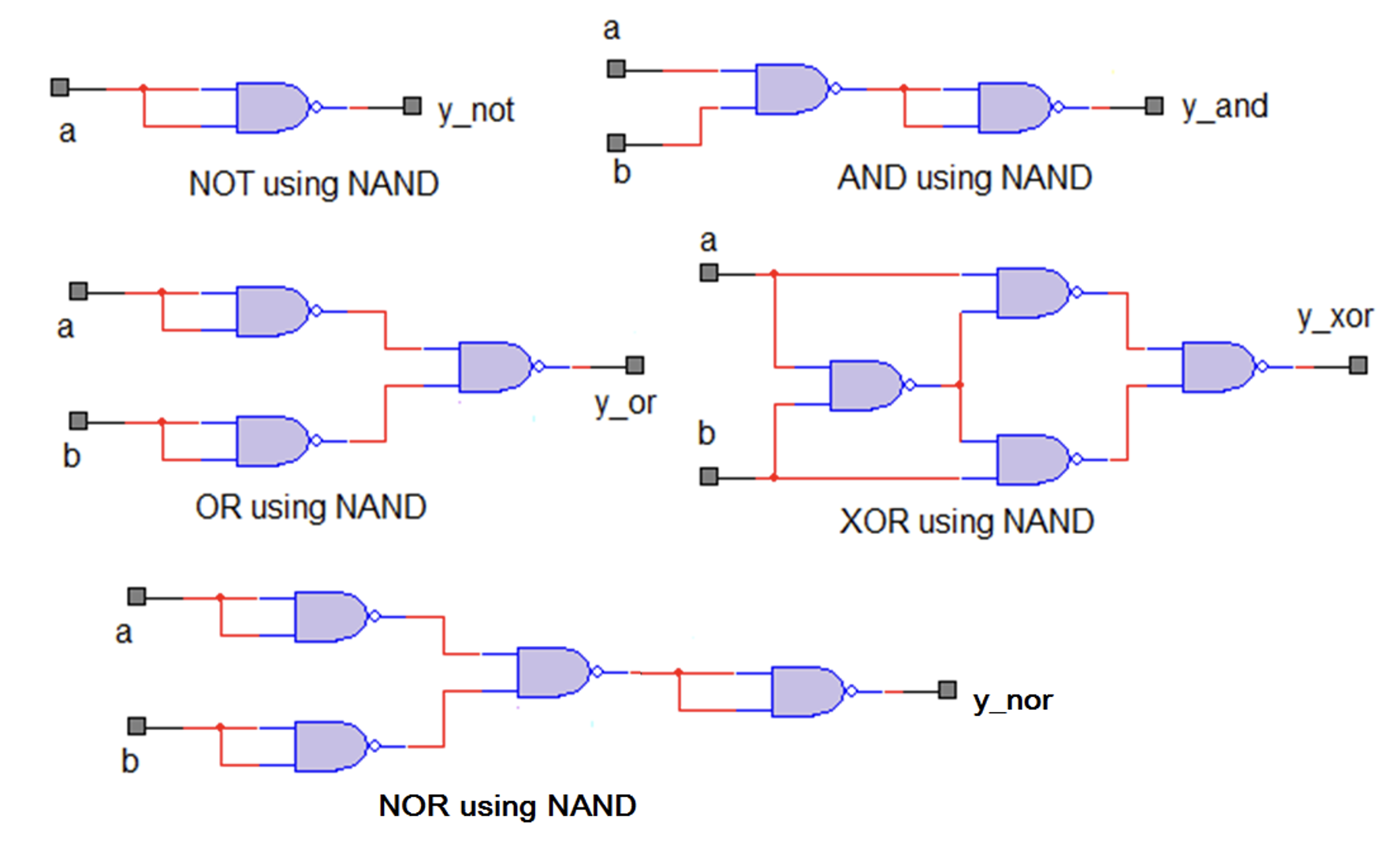
1. NOT Gate from NAND
This is the simplest construction. A NOT gate (or inverter) has one input and one output. We can create it by connecting the two inputs of a NAND gate together.
-
The Logic: A NAND gate's function is
Y = !(A && B). If we tie the inputs so thatA = B, the function becomesY = !(A && A). In Boolean algebra,A AND Ais simplyA. Therefore, the function simplifies toY = !A. This is the definition of a NOT gate. -
The Circuit: Look at the "NOT using NAND" diagram in the image above. A single input
ais wired to both inputs of the NAND gate. The outputy_notwill be the logical inverse ofa.
2. AND Gate from NAND
How do we get an AND gate from something that is "Not AND"? We simply invert the output. An AND gate is a NAND gate followed by a NOT gate.
-
The Logic: We can achieve this by using two NAND gates. The first gate performs the standard NAND operation:
output1 = !(A && B). The second gate is configured as a NOT gate (as we just learned) and takes the output of the first gate as its input:Y = !(output1 && output1), which simplifies toY = !output1. Substituting the first equation into the second gives usY = !(!(A && B)). The double negation!(!X)cancels out, leavingY = A && B. This is the definition of an AND gate. -
The Circuit: Observe the "AND using NAND" diagram. Inputs
aandbgo into the first NAND gate. Its output is then fed into both inputs of a second NAND gate, which acts as an inverter. The final outputy_andis the result ofa AND b.
3. OR Gate from NAND
This construction is the most clever and relies on one of De Morgan's laws, which you may recall from your study of Boolean math. One of these laws states that A || B is equivalent to !(!A && !B).
Let's break down that expression: !(!A && !B).
- We need to invert input
Ato get!A. - We need to invert input
Bto get!B. - We then perform a NAND operation on these inverted inputs.
This gives us a clear recipe for building an OR gate.
-
The Logic: We will use three NAND gates.
- The first NAND gate is configured as a NOT gate for input
A, producing!A. - The second NAND gate is configured as a NOT gate for input
B, producing!B. - The third NAND gate takes the outputs of the first two gates as its inputs, performing the operation
!((!A) && (!B)). By De Morgan's laws, this is equivalent toA || B.
- The first NAND gate is configured as a NOT gate for input
-
The Circuit: The "OR using NAND" diagram shows this exact setup. Input
agoes into its own NAND-based inverter, and inputbgoes into its own. The outputs of these two inverters then become the inputs for the final NAND gate, which produces the OR result aty_or.
To solidify your understanding and see these diagrams again with accompanying explanations, please review the following resource.
Logic NAND Gate Tutorial with NAND Gate Truth Table
This is the same tutorial as before, but now you will focus on the implementation diagrams.
Scroll down to the section titled The "Universal" NAND Gate. Examine the three diagrams under the heading Various Logic Gates. You will see the constructions for NOT, AND, and OR that we have just discussed.
Seeing it in Action
Since your goal is to build a computer in a simulator, it's helpful to see these principles in a simulated environment. The following video demonstrates exactly what we've covered, building the gates in a simple logic simulator.
How to build a computer TUTORIAL
This video from FULXOR shows a practical, hands-on approach to building a computer, starting with the universality of the NAND gate.
First, watch the construction of the NOT gate. Next, see how an AND gate is made by combining a NAND and a NOT. Finally, watch the construction of the OR gate using inverted inputs.
Conclusion
In this lesson, you have demonstrated one of the most elegant concepts in digital logic: the universality of the NAND gate. By combining this single component in different patterns, you have successfully implemented all three fundamental logic functions.
Here are the key takeaways:
- A universal gate is a logic gate that can be used to construct all other logic gates. The NAND gate is a prime example.
- NOT from NAND: Tie the two inputs of a NAND gate together.
!A = !(A && A). - AND from NAND: Invert the output of a NAND gate using a second NAND gate.
A && B = !(!(A && B)). - OR from NAND: Invert both inputs first, then feed them into a NAND gate. This is a practical application of De Morgan's laws.
A || B = !(!A && !B).
You are now equipped with the theoretical and practical knowledge to build any combinational logic circuit you need. In the next lesson, we will put this to use by constructing another essential gate: the XOR gate. This "exclusive OR" gate is the heart of digital addition and will be a critical building block for the Arithmetic Logic Unit (ALU) of your future CPU.