Hello! Welcome to the next lesson in our module on Data Acquisition and DMA.
In our last session, we mastered the fundamental mechanics of the DMA controller by implementing a memory-to-memory transfer. You learned how to configure a DMA channel's source, destination, data width, and increment modes, and how to use an interrupt to signal the completion of the transfer. This was the "Hello, World!" of DMA, proving that we can move data without CPU intervention.
Today, we apply that knowledge to a real-world scenario. Your learning outcome is to configure DMA for a peripheral-to-memory transfer to read ADC results without CPU intervention. This is one of the most common and powerful use cases for DMA in embedded systems. We will move from simply copying memory to offloading a critical data acquisition task from the CPU, which is a vital skill for any firmware engineer.
1. The 'Why': ADC, CPU, and the DMA Solution
Imagine needing to measure a sensor's voltage 1000 times per second.
- Polling Method: Your CPU would be stuck in a tight loop, constantly asking the ADC, "Are you done yet?" This wastes millions of CPU cycles that could be used for other tasks, like processing user input or managing a communication protocol.
- Interrupt Method: This is better. The CPU starts the ADC and goes off to do other work. When the ADC is done, it triggers an interrupt, forcing the CPU to stop, save its context, read the ADC value, store it, restore context, and resume. At 1000 Hz, this context switching adds significant overhead and can still bog down the system.
- DMA Method: The CPU tells the DMA controller: "When the ADC has a new value, please copy it from the ADC's data register directly to this variable in memory." The CPU then starts the ADC and is completely free. The entire transfer happens in the background, handled by dedicated hardware. This is the most efficient method, especially for high-frequency or multi-channel data acquisition.
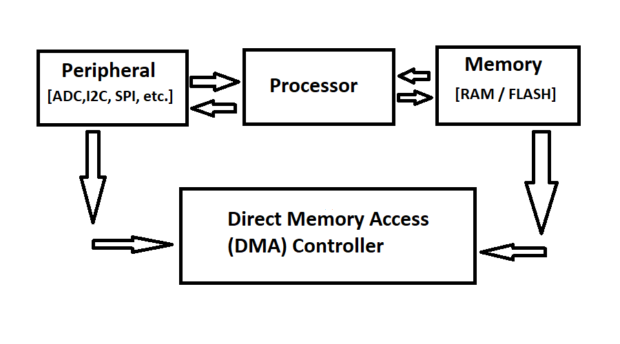
Let's watch a short video to solidify the concept of peripheral-to-memory transfers.
The video 'STM32 DMA PT 1' by Eddie Amaya provides a clear, high-level explanation of the different DMA transfer types. We'll focus on the part that explains peripheral-to-memory transfers.
Watch the following two segments: 00:00 - 04:11: This covers the fundamental purpose of DMA and the three transfer types. Pay close attention to the 'peripheral to memory' explanation. 06:33 - 08:08: This segment conceptually walks through a peripheral-to-memory transfer using a UART example. The logic is identical for an ADC: the peripheral (ADC) signals it has data, which triggers a DMA request to move that data to a memory buffer.
2. Hands-On Lab: Reading an ADC Channel with DMA
It's time to build this system. We will configure the ADC to perform a single conversion and use the DMA to automatically capture the result into a variable.
Step 1: Project Configuration in STM32CubeIDE
- Create a new STM32 project for your
STM32F103C8T6board, or open the one from the previous lesson. - In
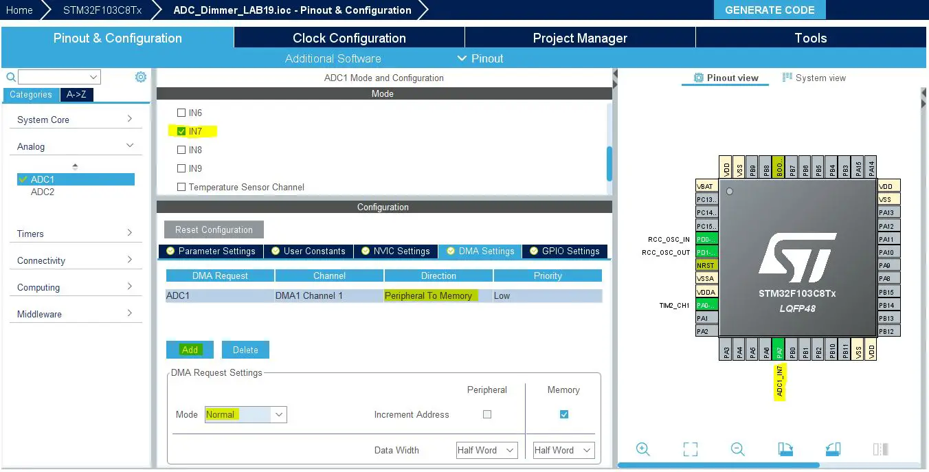
Pinout & Configuration, go to Analog > ADC1. - Check the box for one of the input channels, for example,
IN0. This will assignPA0as an analog input. You can connect the wiper of a potentiometer to this pin to have a variable voltage source. - In the ADC1 configuration pane, under Parameter Settings, you can leave most settings at their default for now.
- Now for the key part. Go to the DMA Settings tab within the ADC1 configuration.
- Click Add and select
ADC1. A DMA channel will be configured for you. - Verify the following settings:
- Direction:
Peripheral To Memory. This is the core of today's lesson. - Mode:
Normal. This tells the DMA to stop after the specified number of transfers is complete. We'll exploreCircularmode in the next lesson. - Increment Address: Check the box for
Memory, but leave the box forPeripheralunchecked. This is critical. We want the DMA to write to sequential locations in our memory buffer (if it were larger than 1), but the source address—the ADC's data register (ADC1->DR)—is fixed and does not change. - Data Width: Set both
PeripheralandMemorytoHalf Word. The STM32F1's ADC has a 12-bit resolution, but the result is stored in a 16-bit (Half Word) data register.
- Direction:
- Go to the NVIC Settings tab and ensure the
ADC1 and ADC2 global interruptis enabled. The HAL uses this interrupt to fire the completion callback after the DMA transfer is done.
- Save the
.iocfile to generate the code.
Step 2: Writing the Application Code
Navigate to Core/Src/main.c. The code is even simpler than our previous memory-to-memory example.
-
In the
/* USER CODE BEGIN PV */section, define a variable to hold the ADC result and a flag to signal completion./* USER CODE BEGIN PV */ uint16_t adc_value; volatile uint8_t conversion_complete_flag = 0; /* USER CODE END PV */Remember, the
volatilekeyword is essential for variables modified within an interrupt and accessed outside of it. -
In the
/* USER CODE BEGIN 4 */section, implement theHAL_ADC_ConvCpltCallback. This weak function is automatically called by the HAL driver when an ADC conversion (including its associated DMA transfer) is complete./* USER CODE BEGIN 4 */ void HAL_ADC_ConvCpltCallback(ADC_HandleTypeDef* hadc) { // This function is called when a conversion is complete and DMA has transferred the result. conversion_complete_flag = 1; } /* USER CODE END 4 */ -
Finally, in
main(), inside thewhile(1)loop, we'll start the conversion and wait for it to complete./* USER CODE BEGIN WHILE */ while (1) { // Reset the flag conversion_complete_flag = 0; // Start the ADC in DMA mode HAL_ADC_Start_DMA(&hadc1, (uint32_t*)&adc_value, 1); // Wait for the conversion to complete while (conversion_complete_flag == 0) { // CPU can do other tasks here... } // For this demo, let's add a delay before the next conversion HAL_Delay(500); /* USER CODE END WHILE */ /* USER CODE BEGIN 3 */ } /* USER CODE END 3 */Let's dissect
HAL_ADC_Start_DMA():&hadc1: A pointer to the ADC handle structure.(uint32_t*)&adc_value: The memory address where the DMA should store the result.1: The number of data items to transfer. Since we are inNormalmode, the DMA will perform one transfer and then stop.
Step 3: Verification with the Debugger
- Place a breakpoint on the
HAL_Delay(500);line. - Build the project and start a Debug Session.
- Add the
adc_valuevariable to the Expressions view. - Resume (
F8) execution. - The code will execute
HAL_ADC_Start_DMA(), which starts the ADC. The CPU will then enter thewhileloop. The ADC will perform its conversion, and upon completion, it will trigger the DMA. The DMA controller will copy the value fromADC1->DRto youradc_valuevariable. Finally, theHAL_ADC_ConvCpltCallbackwill be called, setting your flag and allowing the CPU to break out of thewhileloop. - When execution pauses at your breakpoint, inspect
adc_valuein the Expressions view. You will see a value between 0 and 4095 (since it's a 12-bit ADC). If you have a potentiometer connected, turn it and resume execution to see the value change on the next loop iteration.
You have successfully used the DMA to acquire data from a peripheral with minimal CPU overhead!
3. Under the Hood: From HAL to Registers
Your goal is to become a professional firmware engineer, so it's valuable to understand what the HAL functions are doing at the register level. This knowledge is indispensable for debugging complex issues.
The article below provides an excellent register-level explanation. You don't need to implement it now, but reading through the configuration steps will connect the HAL abstractions to the hardware reality.
STM32 ADC DMA via Registers Tutorial
The article 'STM32 ADC DMA via Registers Tutorial' from ControllersTech walks through a bare-metal implementation. We'll use it to understand the key registers involved.
Read through the sections on ADC and DMA configuration. Focus on understanding the purpose of these registers, which the HAL configures for you: ADC Control Register 2 (ADC1->CR2): Note the DMA bit (Bit 8) that enables DMA requests from the ADC. DMA Configuration Register (DMAx_StreamY->CR): See how direction, circular mode, increment mode, and data size are set. DMA Address Registers (->PAR, ->M0AR): The PAR (Peripheral Address Register) is set to &ADC1->DR, and the M0AR (Memory 0 Address Register) is set to the address of your buffer (&adc_value). DMA Number of Data Register (->NDTR): This is where the transfer count (in our case, 1) is loaded.
By understanding these registers, you can appreciate that HAL_ADC_Start_DMA() is a convenient wrapper that orchestrates the configuration of both the ADC and DMA peripherals to work together seamlessly.
Conclusion
In this lesson, you took a significant step forward by applying your DMA knowledge to a practical data acquisition problem. You have learned how to offload the repetitive task of reading an ADC to the DMA controller, freeing the CPU for more complex work.
Key Takeaways:
- Peripheral-to-memory is the most common and powerful DMA transfer mode.
- The peripheral (ADC) finishing its operation acts as the trigger for the DMA transfer.
- Key configuration details include setting the direction to
Peripheral To Memory, enabling memory address increment, and disabling peripheral address increment. - The
HAL_ADC_Start_DMA()function is the standard HAL call to initiate an ADC conversion sequence that will be handled by the DMA. - The
HAL_ADC_ConvCpltCallback()is the appropriate callback to use for signaling the end of a DMA-managed ADC conversion.
Preview of the Next Lesson:
We've successfully read one channel, one time. But what if you need to continuously monitor multiple sensors? In the next lesson, we will set up the ADC in scan mode with DMA to continuously acquire data from multiple channels. We will switch the DMA to Circular mode, a powerful technique that allows for creating a seamless, endless data acquisition pipeline.