Hello! Welcome back.
In our last lesson, you successfully set up your complete professional toolchain. You established the physical and software link between your computer and the STM32 microcontroller by creating and flashing an empty project. That connection is the pathway we'll use for everything that follows.
Today, we move from the "how" of connecting to the "what" and "where" of programming. This lesson addresses the learning outcome: Describe the ARM Cortex-M3 architecture and the STM32F103 memory map. We will explore the "brain" of your microcontroller—the CPU core architecture—and the "city plan" it uses to find its way around—the memory map. This is the foundational knowledge that separates a firmware engineer from a coder; you'll understand the machine you're commanding at its fundamental level.
1. The Core of the Machine: ARM Cortex-M3 Architecture
Your STM32F103 microcontroller is built around a processor core designed by ARM, called the Cortex-M3. Think of this as the central processing unit (CPU) of the chip. It fetches your program instructions from memory, executes them, performs calculations, and manages the flow of data.
Let's look at its key characteristics.
This document from a standard textbook provides a formal overview of the Cortex-M3 processor. We'll use it to understand the core's fundamental design.
Please read the section '2.1 Fundamentals'. Focus on the description of the Cortex-M3 as a 32-bit processor with a Harvard architecture.
As you read, the two most important takeaways are:
- 32-bit Processor: The Cortex-M3 is designed to work with data in 32-bit chunks (4 bytes). Its internal pathways (data paths) and storage locations (registers) are 32 bits wide.
- Harvard Architecture: It has separate buses for instructions and data. This is a performance optimization that allows the processor to fetch the next instruction while simultaneously reading or writing data for the current instruction.
The CPU's Internal Registers
Inside the Cortex-M3 core are a small number of extremely fast memory locations called registers. These are the CPU's immediate scratchpad for all its work.
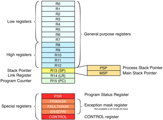
Here are the most important ones for you to know, as detailed in the "Overview of the Cortex-M3" document under section 2.2 ("Registers"):
- General-Purpose Registers (R0-R12): Used for data manipulation, calculations, and temporarily storing values.
- Stack Pointer (R13 or SP): This is a crucial register that always holds the memory address of the "top" of the stack. The stack is a region in RAM used to store local variables, function parameters, and return addresses when you call a function. The Cortex-M3 actually has two stack pointers (Main and Process), which is a feature used by operating systems, but for now, just think of it as the manager of your program's temporary memory.
- Link Register (R14 or LR): When your code calls a function, the CPU needs to know where to return to when the function is finished. The address of the next instruction is automatically stored in the Link Register before jumping to the function.
- Program Counter (R15 or PC): This is perhaps the most important register. It always contains the memory address of the next instruction the CPU will execute. As the CPU runs your code, the PC automatically increments, stepping through your program one instruction at a time.
These registers are the heart of the processor's state. When we use a debugger, we are often "peeking" inside the chip to see the values held in these very registers.
2. The Landscape: The STM32 Memory Map
Now that you've seen the CPU core, let's look at how it views the rest of the system. The Cortex-M3 architecture uses a single, unified 4-gigabyte address space. This means every single component—the Flash memory holding your code, the SRAM holding your variables, and all the hardware peripherals like GPIO, UART, and I2C—is accessible at a specific address in this vast space.
This concept is called Memory-Mapped I/O. It's a powerful design because it means we don't need special CPU instructions to talk to hardware. We can simply read from or write to a specific memory address using standard C pointers.
This video gives a concise and clear explanation of Memory-Mapped I/O, which is the central principle for controlling all peripherals on an STM32.
Watch the first part of the video, from 00:00 to 01:27. Pay close attention to the idea that we can use normal 'load' and 'store' operations (which in C correspond to reading from and writing to pointers) to control hardware.
The Major Regions
This 4GB space is organized into predefined regions. While the ARM standard defines the layout, STMicroelectronics customizes it for the specific peripherals included in the STM32F103.

Let's look at the most important regions for our work, which are consistent across most Cortex-M devices:
| Memory Region | Starting Address (STM32F103) | Size (STM32F103C8T6) | Purpose & Characteristics |
|---|---|---|---|
| Code (Flash) | 0x08000000 |
64KB or 128KB | Stores your compiled program code. Non-volatile (retains data after power-off). |
| SRAM | 0x20000000 |
20KB | Stores program variables, the stack, and the heap. Volatile (loses data on power-off). |
| Peripherals | 0x40000000 |
512MB | Contains the registers for all hardware modules (GPIO, Timers, UART, SPI, I2C, CAN, ADC, etc.). |
| System | 0xE0000000 |
512MB | Contains core-related peripherals like the NVIC (interrupt controller) and SysTick timer. |
This structure is what allows you to write C code that directly interacts with hardware. When you want to turn on an LED, you are simply writing a specific value to a specific address inside the "Peripherals" memory region.
3. Finding Your Way: Datasheets and Reference Manuals
So, how do you find the exact address for the GPIO register that controls a pin? This is where two documents become an embedded engineer's most critical tools: the Datasheet and the Reference Manual.
Interrupts and Memory Mapped I/O :: Bare Metal Programming Series 2
Knowing which document to consult is a key professional skill. This video explains the role of each document.
Watch the segment from 01:55 to 05:25. The speaker does an excellent job explaining why both the datasheet and the reference manual are your 'source of truth'.
In summary:
- Datasheet (DS): Provides high-level electrical and physical characteristics. Think of it as the chip's "spec sheet" with pinouts, voltage ratings, and a general feature list. It contains the high-level memory map diagram.
- Reference Manual (RM): Provides the detailed information needed by application developers. It describes the functionality of each peripheral and, most importantly, lists all the memory-mapped registers, their addresses, their individual bits, and what each bit does. This is your primary guide for programming.
Let's trace an example: To enable the GPIO Port C peripheral, you must first enable its clock in the Reset and Clock Control (RCC) peripheral.
- The memory map tells us the RCC peripheral registers begin at address
0x40021000. - The STM32F103 Reference Manual (document RM0008) tells us in the RCC section that the register to enable GPIO clocks is the
APB2ENRregister. - The manual specifies that
RCC_APB2ENRhas an offset of0x18from the RCC base address. - Therefore, the absolute memory address of the
RCC_APB2ENRregister is0x40021000 + 0x18 = 0x40021018. - The manual further shows that to enable Port C, we need to set bit 4 (the
IOPCENbit) in that register to 1.
This process of looking up base addresses and register offsets in the reference manual is a fundamental daily task for a firmware engineer.
Test your understanding!
Using the memory map image provided earlier, you can see that the base address for the GPIOA peripheral is 0x40010800. The reference manual for the STM32F103 states that the "Port output data register" (ODR) is at offset 0x0C from the peripheral's base address.
What is the absolute memory address for the GPIOA ODR register?
Show answer
The absolute address is the base address plus the offset:0x40010800 + 0x0C = 0x4001080C.
To write data to the pins of Port A, your program will need to write a value to this specific memory address.
4. The Beginning of Everything: The Boot Process
We now know the CPU has registers and the system has a memory map. But when you apply power, how does the CPU know where to find the start of your program?
This is handled by a hardware-defined boot sequence.
C Bare Metal Programming on STM32F103 — Booting up
This article explains the boot process in a very clear way, solving the 'chicken-and-egg' problem of how a program starts.
Read the sections that explain the 'Reset exception', the 'vector table', and 'Memory maps' (aliasing). This explains how the hardware knows where to find the first instruction of your code.
Here is the sequence of events when your Blue Pill powers on:
- Reset: The processor enters a "Reset" state.
- Vector Table Fetch: The hardware is designed to look at a fixed memory location,
0x00000000, which is the start of the vector table. The vector table is essentially a list of starting addresses for critical functions (exception handlers). - Initialize Stack Pointer: The very first 32-bit value at address
0x00000000is loaded into the Stack Pointer (SP) register. This sets up the program's stack in RAM. - Initialize Program Counter: The second 32-bit value at address
0x00000004is the address of the Reset Handler function. This value is loaded into the Program Counter (PC). - Execution Begins: The CPU now begins execution at the address held in the PC, which is the start of your program's initialization code.
But wait, we know our program is stored in Flash memory, which starts at 0x08000000. How can the CPU read from 0x00000000?
The STM32 has a clever feature: by default, on boot-up, it aliases the Flash memory. This means the memory content at 0x08000000 is also made visible at 0x00000000. The CPU thinks it's reading from address zero, but it's actually reading the very beginning of your firmware binary stored in Flash. This is how the linker, the compiled code, and the hardware all work together to start your application.
Conclusion
In this lesson, we've moved from a black box to a detailed blueprint of your microcontroller. You should now be able to describe the fundamental components and their layout.
Key Takeaways:
- The ARM Cortex-M3 is a 32-bit CPU core with key registers like the Program Counter (PC) and Stack Pointer (SP) that manage program flow and memory.
- All components on the STM32 exist in a single 4GB memory map, and we control hardware peripherals using Memory-Mapped I/O—writing to and reading from specific addresses.
- The Reference Manual is your indispensable guide to finding the addresses and functions of peripheral registers.
- The boot process relies on a vector table at the beginning of your firmware in Flash, which the hardware uses to initialize the SP and PC and begin execution.
Preview of the Next Lesson:
Now that we know where the peripheral registers are, our next step is to learn how to talk to them safely and precisely using the C language. In the next lesson, we will cover the essential tools for register-level programming: bitwise operators, fixed-width integers, and the crucial volatile keyword. We will then combine this knowledge to write our first bare-metal program that directly manipulates a GPIO register to blink an LED.