Introduction
In our previous lesson, we explored the internal architecture of the ARM Cortex-M processor—its registers, operating modes, and execution model. We established a model of the CPU as the "brain" of the microcontroller. Now, we'll zoom out to see the world from the CPU's perspective: the memory map. This is the blueprint that tells the processor where everything is located, from the code it needs to execute, to the data it needs to manipulate, to the hardware peripherals it needs to control.
This lesson directly addresses our next learning outcome: to identify the memory regions (Flash, SRAM, and peripherals) in an STM32 memory map. For a software engineer, understanding the memory map is the critical link between the abstract world of code (variables, functions, objects) and the physical reality of the hardware. It explains how writing GPIOA->ODR = 1; actually manipulates a physical pin and why some variables retain their value after a power cycle while others vanish.
What is a Memory Map?
At its core, a processor does two things: it performs computations and it moves data. To do this, it needs to be able to access memory and peripherals. In the ARM Cortex-M architecture, these are not treated as separate entities. Instead, everything—program memory, data memory, and hardware peripherals—is located in a single, unified address space. Since the Cortex-M is a 32-bit processor, it can address bytes, which gives it a 4-gigabyte (GB) address space, from address 0x00000000 to 0xFFFFFFFF.
The memory map is a chart that defines which addresses correspond to which hardware components. This architecture uses a concept called memory-mapped I/O. This means that to interact with a peripheral, like a GPIO port or a UART, you simply read from or write to the specific memory addresses assigned to that peripheral's control registers. There are no special I/O instructions; it's all just memory access.
The LinkedIn article "STM32 Memory Map Explained" by David Zhu provides an excellent high-level overview of this concept and the typical layout.
STM32 Memory Map Explained: Where Your Code Lives 🗺️
This article offers a clear, structured introduction to the STM32 memory map.
Please read the introductory sections "What is a Memory Map?" and "The STM32 Memory Map Overview". Then, jump to the end and read the summary under "Key Takeaways". This will give you a solid frame of reference for the details that follow.
The Major Memory Regions
The 4GB address space of an STM32 microcontroller is divided into several large, standardized blocks. While the exact size and contents of each block vary between different STM32 models, the overall structure is consistent.
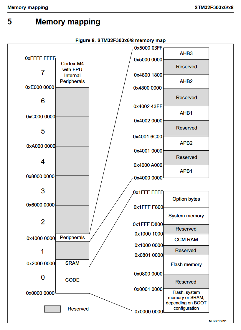
As you can see, the main regions of interest to us are:
- Code Region: Primarily holds the on-chip Flash memory.
- SRAM Region: On-chip Static RAM for runtime data.
- Peripheral Region: Where the control registers for hardware like GPIO, Timers, UART, SPI, etc., are located.
- Cortex-M Core Peripherals: A special region for peripherals that are part of the ARM core itself, like the Nested Vectored Interrupt Controller (NVIC) and the SysTick timer, which we'll cover later.
Let's examine each of these in more detail.
1. Flash Memory (Code)
Flash memory is the primary storage for your program. Its key characteristics are:
- Non-volatile: It retains its contents even when the power is turned off. This is where your compiled firmware is permanently stored.
- Read-mostly: While you can write to Flash programmatically, it's a much slower and more complex operation than writing to RAM. During normal execution, it's treated as read-only.
- Slower than SRAM: Accessing instructions or data from Flash requires "wait states," which are small delays the CPU must insert to allow the Flash memory to catch up.
On most STM32 devices, the main Flash memory starts at address 0x08000000. The processor fetches and executes instructions directly from this address. This capability is known as Execute In Place (XIP), and it's a fundamental feature of modern microcontrollers, as it saves having to copy the entire program into the much smaller and more precious SRAM before execution.
2. SRAM (Data)
SRAM, or Static Random-Access Memory, is your workspace. Its characteristics are the inverse of Flash:
- Volatile: It loses all its contents when power is removed.
- Read/Write: It is designed for fast and frequent reading and writing.
- Fast: It operates at the full speed of the CPU, typically with zero wait states.
SRAM is where all your runtime data lives: global variables, the stack (for local variables and function calls), and the heap (for dynamic memory allocation). On most STM32s, the main SRAM block starts at address 0x20000000.
3. Peripherals
This large region of the memory map, typically starting around 0x40000000, is dedicated to controlling the microcontroller's hardware peripherals. Each peripheral is assigned a block of addresses. Within that block, individual registers control specific aspects of the peripheral's behavior.
Think of it as a giant switchboard. If you want to set pin 5 of GPIO Port A high, you write a 1 to the correct bit in a specific register located at a precise address within the GPIOA address block. The blog post "Lets look inside!" from ciesie.com explains this concept well. It describes the memory space as a "row of switches" you can flip to control the hardware.
The peripheral region itself is further organized by buses, such as the AHB (Advanced High-performance Bus) and APB (Advanced Peripheral Bus). These buses connect groups of peripherals to the processor core. You can see this structure in the video below, which walks through a device's reference manual.
Datasheet and Reference Manual Overview: STM32 Bare Metal Software from scratch #2
This video from AsabreTech demonstrates how to find and interpret the memory map in an official STM32 reference manual, connecting the abstract map to the physical hardware buses.
Please watch from this segment. The presenter shows the memory map diagram and explains how the peripheral addresses are grouped by the APB and AHB buses shown in the device's block diagram. This reinforces that the memory map isn't arbitrary; it reflects the physical architecture of the chip.
The Software View: How Code and Data Are Organized
So far, we've discussed the hardware memory regions. As a software engineer, you're likely more familiar with logical memory sections like .text (code), .data (initialized variables), .bss (uninitialized variables), the stack, and the heap. How do these software concepts map onto the physical Flash and SRAM?
This is where the compiler and linker come in. They work together to place these logical sections into the appropriate physical memory regions. The following diagram provides an excellent visualization of this process.

Let's break down what this diagram shows:
- .text, .rodata: The executable code (
.text) and read-only constant data (.rodata) are placed in Flash memory. They are executed directly from Flash (XIP). - .data: This section contains global and static variables that have an initial value (e.g.,
int counter = 100;). These initial values must be stored permanently, so they reside in Flash. However, to be modified at runtime, the variables must be in RAM. Therefore, at startup, a small piece of code copies the contents of the.datasection from Flash to SRAM. In the diagram, the Flash location is the Load Memory Address (LMA), and the SRAM location is the Virtual Memory Address (VMA). - .bss: This section is for global and static variables that are uninitialized or initialized to zero (e.g.,
int buffer[1024];). Since their initial value is zero, there's no need to store a block of zeros in Flash. The linker simply reserves space for this section in SRAM, and the startup code clears this memory region to zero beforemain()is called. - Heap: This is an area of SRAM available for dynamic memory allocation (e.g., using
malloc()). It typically grows "upwards" from the end of the .bss section. - Stack: This area of SRAM is used for function call frames, local variables, and saving processor state during interrupts. It is placed at the very top of SRAM and grows "downwards".
The following video offers a clear explanation of these different memory sections and the critical relationship between the stack and the heap.
Memory Layout in Embedded Systems | Flash, RAM, Stack, Heap Explained with STM32
This video from TechVedas .learn provides a detailed explanation of the logical memory layout inside Flash and RAM.
Watch the segment from this point, which covers Flash memory, RAM, and the .data, .bss, heap, and stack sections. Pay close attention to the distinction between where variables are stored (LMA) and where they are used (VMA), and the potential for stack/heap collision.
Conclusion
In this lesson, we have mapped out the memory landscape of an STM32 microcontroller. Understanding this map is not just an academic exercise; it's fundamental to every aspect of embedded development, from debugging and optimization to writing robust, reliable firmware.
Here are the essential takeaways:
- Unified Address Space: STM32 microcontrollers use a memory-mapped architecture where code, data, and peripherals all reside in a single 4GB address space.
- Physical Memory Regions: The primary hardware regions are Flash memory (non-volatile, for code and constants, starting at
0x08000000), SRAM (volatile, for runtime data, starting at0x20000000), and the Peripheral region (for hardware control via memory-mapped registers). - Logical Software Sections: The linker organizes your program into logical sections (
.text,.data,.bss) and places them into the physical memory. The.datasection is a key example, being stored in Flash (LMA) and copied to SRAM (VMA) at startup. - Stack and Heap: These dynamic regions reside in SRAM and grow towards each other, making stack overflow a critical concern in resource-constrained systems.
With this knowledge of the processor's architecture and its view of memory, we are now ready to tackle a crucial process: the boot sequence. In the next lesson, we will trace the journey of the microcontroller from the moment it powers on, through the initial setup code, to the very first line of your main() function. This will connect the dots between the memory map and the processor's execution flow.