Recommended resources
The freely available resources this lesson will direct you to.
Introduction
Welcome back. In our previous lesson, we established a critical concept: for many modern AI workloads, particularly the autoregressive decoding phase of large language models, performance is not limited by computation but by memory bandwidth. We saw how even the most powerful GPUs can sit mostly idle, waiting for data to be moved from their main memory. This firmly established why memory bandwidth is a paramount concern in AI system design.
Today, we transition from the "why" to the "how." This lesson addresses the technologies engineered to solve the bandwidth problem. Your goal for this lesson is to compare High Bandwidth Memory (HBM) and GDDR memory technologies in terms of their performance, power, and cost tradeoffs.
By the end of this lesson, you will understand the fundamental architectural trade-offs between these two dominant memory solutions for GPUs. This knowledge is essential for evaluating hardware choices and understanding the design decisions behind high-performance accelerators like the NVIDIA H100 versus a consumer-grade RTX 4090.
1. The Core Dichotomy: Wide & Slow vs. Narrow & Fast
At the heart of the HBM vs. GDDR debate is a fundamental difference in design philosophy for achieving high bandwidth.
- High Bandwidth Memory (HBM) follows a "wide and slow" approach. It uses an extremely wide data bus (e.g., 1024 bits or more) running at a relatively modest clock frequency.
- Graphics Double Data Rate (GDDR) memory, in contrast, follows a "narrow and fast" approach. It employs a much narrower data bus (e.g., 256 or 384 bits) but drives signals at very high frequencies (many gigabits per second per pin).
To understand how these different philosophies are realized physically, let's watch a short video that provides an excellent overview.
This video from Semiconductor Engineering clearly illustrates the architectural differences between an HBM and a GDDR6 system designed to achieve the same total bandwidth. Focus on how the physical structure enables each approach.
Watch the segment from 01:13 to 03:16. Pay attention to the description of the HBM system with its 1024-bit interface and 2.5D interposer, and contrast it with the GDDR6 system using fewer, faster pins on a traditional board.
The video introduces the key physical enablers for each technology:
HBM: 3D Stacking and the Interposer
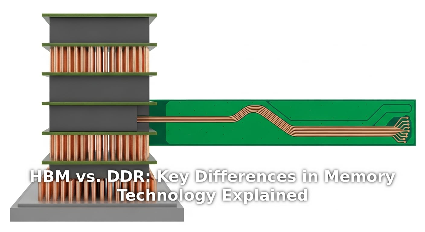
HBM achieves its massive bus width by moving into the third dimension. Instead of placing memory chips side-by-side on a circuit board, HBM stacks multiple DRAM dies vertically. These dies are connected by thousands of microscopic vertical wires called Through-Silicon Vias (TSVs).
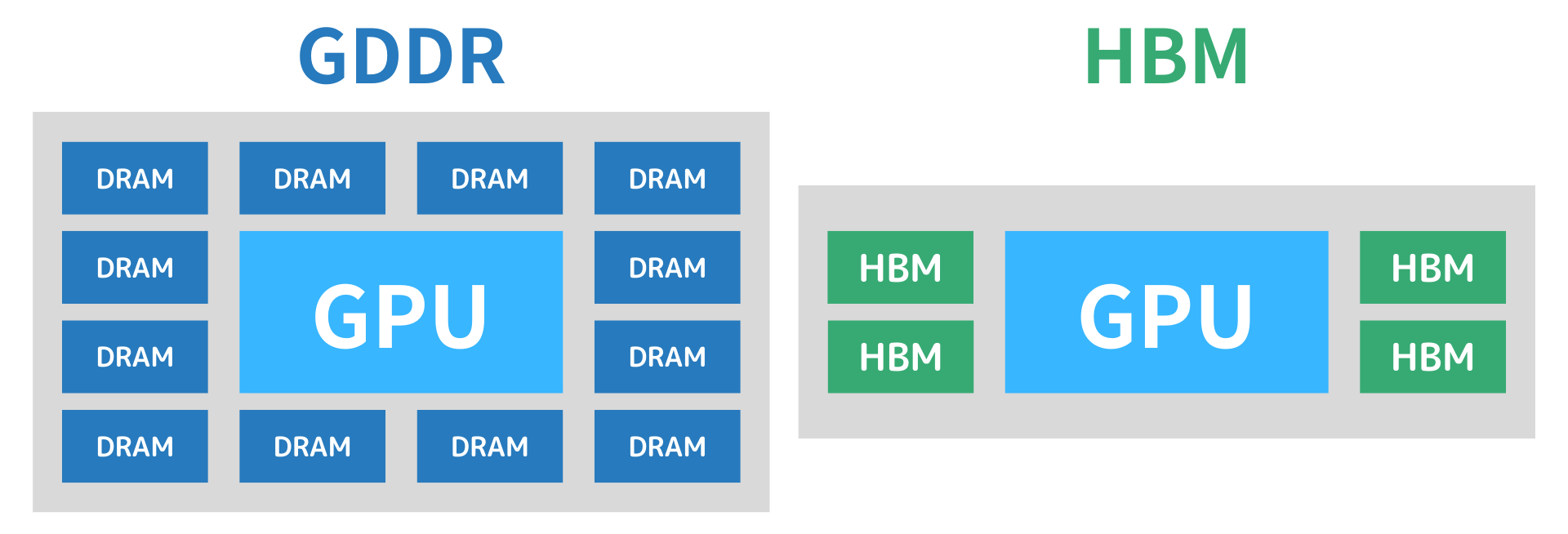
This entire memory stack is then placed very close to the GPU die on a special silicon base layer called an interposer. This entire assembly (GPU + HBM stacks on an interposer) is packaged together. This is often called 2.5D packaging.
GDDR: Planar Design on a PCB
GDDR uses a more traditional 2D, planar approach. Individual GDDR memory chips are soldered onto the main Printed Circuit Board (PCB) surrounding the GPU. The connections are longer traces running across the board. Signal integrity challenges over these longer distances fundamentally limit how wide and fast the bus can be, which is why GDDR relies on pushing the frequency of a narrower set of connections to its limits.
2. A Deep Dive into the Trade-offs
Now that we understand the architectural foundations, let's systematically analyze the trade-offs across performance, power, and cost. For a comprehensive technical breakdown, we'll use the following detailed report as our primary reference.
[PDF] HBM vs. DDR: Key Differences in Memory Technology Explained
This PDF provides an in-depth technical analysis comparing HBM and DDR/GDDR technologies. It contains detailed specification tables and explanations that will form the basis of our comparison.
Please read the following parts of the document: Table 1 (page 3): This gives a fantastic at-a-glance comparison of DDR5 and HBM3 specs. Section 'DDR vs HBM: Key Differences' (starts on page 6): Read this section carefully. It methodically breaks down the contrasts in bandwidth, capacity, power, latency, and packaging. Table 2 (page 8): This table provides a concise, high-level summary of the trade-offs. The final table, titled 'Representative Memory Configurations' (page 12), shows how these memory types are used in real-world products like the NVIDIA H100 and AMD MI300A.
Let's synthesize the information from this report and our other resources into a clear comparison.
| Metric | High Bandwidth Memory (HBM) | GDDR (e.g., GDDR6/6X) |
|---|---|---|
| Philosophy | Wide & Slow: Achieves bandwidth via a massive bus (1024-4096 bits). | Narrow & Fast: Achieves bandwidth via high data rates per pin (16-24 Gbps). |
| Bandwidth | Extremely High. A single HBM3 stack offers >800 GB/s. A multi-stack GPU (like an NVIDIA H100) can exceed 3 TB/s. | High. A full card implementation (e.g., RTX 4090) can achieve ~1 TB/s. |
| Power Efficiency | Higher. Shorter, on-interposer traces and lower clock speeds per pin result in lower energy-per-bit transferred. A key advantage in datacenters. | Lower. Driving high-frequency signals over longer PCB traces consumes significantly more power. |
| Cost & Complexity | Very High. Requires complex 3D stacking (TSVs), a costly silicon interposer, and advanced 2.5D packaging. Manufacturing yields are lower. | Lower. Uses mature, commoditized 2D PCB technology and standard chip packaging. Much simpler and cheaper to integrate. |
| Capacity | Lower per stack. HBM stacks are typically 8-24 GB. While a GPU can have multiple stacks, total capacity is often a design constraint. | More flexible. Easier to place more discrete chips on a board to achieve higher total capacities (e.g., 24 GB is common on high-end consumer cards). |
| Physical Footprint | Smaller. The 2.5D packaging is very compact, enabling higher bandwidth density (GB/s per mm²). | Larger. Spreading discrete chips around the GPU on a PCB consumes more board area. |
| Thermal Issues | Challenging. The close proximity of memory to the hot GPU die requires sophisticated and integrated cooling solutions. | Simpler. Memory chips are more distributed on the PCB, making it easier to cool them independently of the GPU. |
To further solidify your understanding of these trade-offs from an engineering perspective, the following video provides a quantitative look at the SoC (System-on-Chip) level.
This video, also from Semiconductor Engineering, features a different expert who quantifies the differences in silicon area and power consumption for the PHY (the physical interface circuitry on the GPU die) needed for GDDR6 vs. HBM2.
Watch the final segment starting at 09:04. The speaker breaks down a 256 GB/s implementation, comparing pin counts, data rates, PHY area, power consumption, and the added cost of the interposer for HBM.
The key figures from the video are striking: for the same total bandwidth, a GDDR6 interface requires 1.5x-1.75x more silicon area and consumes 3.5x-4.5x more power on the GPU die compared to an HBM interface. This comes at the cost of the HBM system's expensive interposer and more complex manufacturing.
3. Application and Market Segmentation
These trade-offs directly dictate where each memory technology is deployed. The choice is a classic engineering decision balancing performance requirements against cost and power budgets.
- HBM is the choice for high-end datacenter AI accelerators. For workloads like training massive models or serving LLMs at scale (where the memory-bound decode phase dominates), absolute memory bandwidth and power efficiency are paramount. The high cost is justified by the performance gains and lower operational power costs (TCO). This is why you see HBM3 on the NVIDIA H100 and AMD MI300X.
- GDDR is the choice for consumer graphics and cost-sensitive professional applications. For gaming, content creation, and even smaller-scale AI workloads, GDDR provides an excellent balance of high performance at a manageable cost. The bill of materials for a consumer GPU must be kept in check, making HBM's high cost prohibitive. This is why the powerful GeForce RTX 4090 uses GDDR6X.
The report HBM vs. DDR: Key Differences in Memory Technology Explained gives concrete examples in its table of "Representative Memory Configurations," showing the clear split between datacenter (HBM) and consumer (GDDR) products.
Conclusion
In this lesson, we dissected the two leading memory technologies for high-performance computing, connecting their physical architectures to their distinct profiles of performance, power, and cost.
Key Takeaways:
- HBM achieves its industry-leading bandwidth through a "wide and slow" architecture, enabled by 3D die stacking and 2.5D packaging on a silicon interposer.
- GDDR uses a traditional planar "narrow and fast" architecture, pushing frequencies on a standard PCB to deliver a cost-effective high-performance solution.
- The primary trade-offs are clear:
- Performance: HBM offers significantly higher raw bandwidth (>3 TB/s vs. ~1 TB/s).
- Power: HBM is substantially more power-efficient per bit transferred.
- Cost: GDDR is dramatically cheaper and less complex to manufacture and integrate.
- This leads to a market segmentation where HBM dominates the cost-insensitive, performance-at-all-costs datacenter market, while GDDR excels in the cost-sensitive consumer and prosumer markets.
Preview of the Next Lesson:
We have now built a strong foundational understanding of the GPU's architecture, from its parallel processing model (SIMT) and scheduling (warps) to its memory hierarchy and the physical memory technologies themselves. The next logical step is to bridge the gap from hardware to software.
In our next lesson, we will begin Module 3 by diving into the CUDA programming model. We will explore its core abstractions—grids, blocks, and threads—and see how these software concepts map directly onto the hardware components we've spent the last two modules examining. This will be your first step toward understanding how to command the immense power of these parallel processors.