Recommended resources
The freely available resources this lesson will direct you to.
Hello! This first module builds a platform map before moving into power sequencing, schematics, and fault diagnosis. Today you will construct a functional block diagram of an x86-64 laptop: which components are present, which connect directly, and what each connection is for. The goal is not to memorize one motherboard layout. It is to make a diagram you can adapt when a real board integrates, relocates, or omits a component.
Start with two centers of activity
A laptop has more than one important processor. The CPU runs the main system software and contains the memory controller on the representative platforms we will study. The embedded controller (EC) is a separate microcontroller concerned with laptop-specific management, such as the power button, keyboard, battery-related functions, and fans. Between the CPU and many peripheral devices sits I/O logic commonly called a chipset; in a two-chip Intel design, its principal chip is the Platform Controller Hub (PCH).
Watch the short architectural explanation below. It uses desktop motherboards as examples, so concentrate on the connection pattern, not the physical shape of the board.
Explaining Motherboard Chipsets
“Explaining Motherboard Chipsets” from ExplainingComputers shows why modern diagrams place memory and some high-speed connections at the CPU, while other I/O connections belong to a chipset.
Watch the historical comparison to see which older northbridge functions moved into the CPU. Continue with the modern layout; notice the CPU’s direct memory and PCIe connections and the Intel DMI link to the chipset.
The distinction matters whenever you draw a line. RAM should not be placed behind the PCH merely because the PCH is described as an “I/O hub.” Conversely, a device connected through the PCH still communicates with the CPU; the diagram shows where its controller or physical link attaches, not whether the CPU can use it.
Place memory, chipset, and storage
Intel’s Introduction to Intel Architecture, The Basics provides a useful two-chip example. Its processor and PCH are representative components, not a specification for every current laptop: the example uses older hardware, and some laptop designs integrate PCH functions into the processor package or system-on-chip.
[PDF] White Paper: Introduction to Intel® Architecture, The Basics
Read Intel’s platform overview to establish which links belong near the CPU and which belong near the PCH.
In “Basics of an Intel Architecture System” (printed p. 5), read the platform overview. Pay attention to the two-chip design and its single-chip exception. In “Intel Core i7 Processor-Based System” and “The Intel Core i7 Processor” (printed p. 6), read the processor features. Then, in “Intel’s Direct Media Interface (DMI)” (printed pp. 6–7), locate the explanation beginning “DMI is the name given to the link”; focus on why it is a link between the processor and PCH. In “Platform Controller Hub (PCH)” and “Modern I/O Interfaces” (printed pp. 7–8), read the interface list, then the SPI description. Note SATA for storage, SPI for firmware flash, and LPC as a low-speed interface.
Start your diagram with DRAM connected directly to the CPU by a DDR or LPDDR memory interface. DDR and LPDDR describe families of memory interfaces; a particular board uses the type its processor and memory design support. The CPU’s integrated memory controller manages that connection. This is why “RAM” is a block beside the CPU, not a branch hanging from the storage controller.
Next, connect the CPU to the PCH. Label that link DMI if you are drawing the representative two-chip Intel architecture. “Chipset” is a useful functional label, but DMI is Intel-specific; do not copy it onto every x86-64 design.
Storage requires a more careful choice of line than the word “SSD” suggests:
- A SATA SSD connects to a SATA controller, commonly shown at the PCH in this model.
- An NVMe SSD communicates over PCI Express (PCIe). Its PCIe connection may come from CPU lanes or from chipset lanes, depending on the board.
Thus, NVMe names the storage protocol and PCIe names the connection you should label on the diagram. “M.2” alone is not enough to identify that connection: it describes a connector and card form factor, not a single bus. Show the storage arrangement of the platform you mean to describe rather than drawing every possible SSD as though it were installed.
Add the laptop-specific control and firmware blocks
The EC deserves its own box. It can be active when the main CPU is not running, which is essential to its role in responding to the power button and supervising laptop functions. The following clip introduces that role; treat its examples as typical functions, not a claim that every EC implements charging or thermal control identically.
“EC and BIOS explanation demo” from The Chipmaster introduces the embedded controller as a microcontroller and identifies several functions that distinguish a laptop diagram from a simple CPU-and-chipset sketch.
Watch the EC introduction. Focus on its relationship to the power button, indicators, fans, keyboard, and battery-related management. We will examine the actual ordering of power and reset signals in the next lesson.
The curated laptop image is a good test of what a block diagram can—and cannot—tell you.
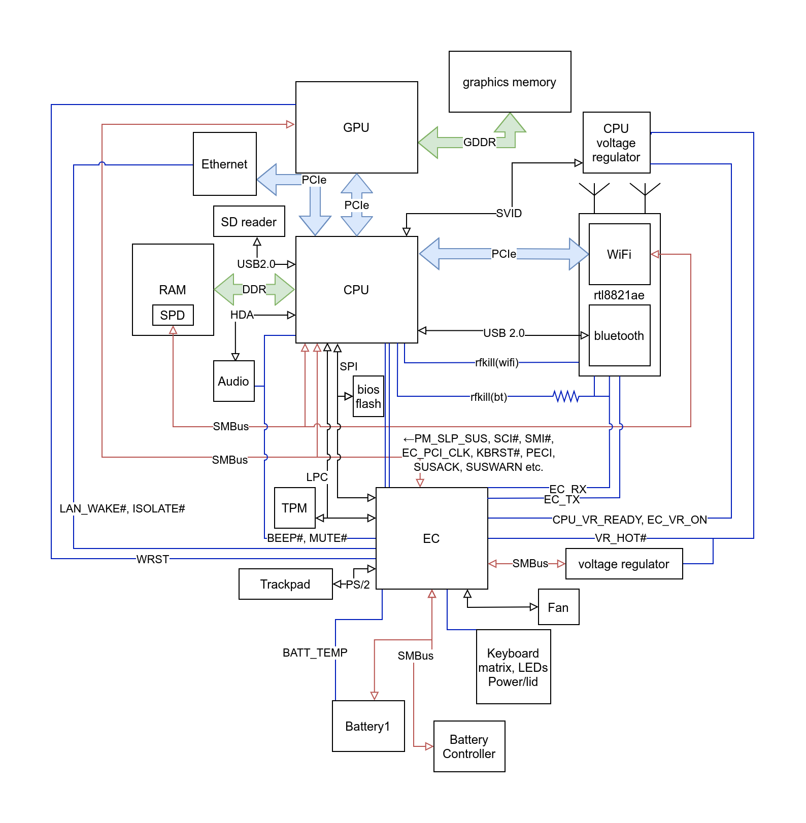
The image brings the EC into view, along with its relationships to the keyboard, fan, battery-related circuitry, and main platform. It also illustrates a limitation of simplified diagrams: a line that reaches a “CPU” box may represent an integrated controller or omit an intervening I/O block. Do not infer that every laptop has no PCH simply because this drawing does not show one. Equally, add storage to your diagram even though this particular image leaves it out.
Now give three easily confused blocks distinct jobs:
SPI flash is nonvolatile storage for platform firmware, including the code commonly called BIOS or UEFI firmware. In the representative two-chip Intel design, draw it at the PCH’s SPI controller and label the link SPI. Unlike a drive containing the operating system and user files, this chip holds code the platform needs for initialization. Calling it “ROM” does not mean that it can never be rewritten.
The TPM supports security functions such as protected keys and measurements. It is not the chip that normally stores the UEFI firmware image. A discrete TPM may have a low-speed connection such as LPC or SPI, depending on the design. Some platforms instead implement TPM functionality within another platform component; in that case, do not invent a separate physical TPM chip.
The EC has its own firmware and management responsibilities. In a representative diagram, connect it to the PCH or integrated platform I/O logic using the appropriate board interface, such as eSPI on many newer designs or LPC on older ones. Its other connections need not all be drawn as data buses: a power-button input or fan-control output is a control signal, while SMBus can be used for communication with battery-related devices. EC firmware might be stored internally, separately, or under a board-specific flash-sharing arrangement. A generic diagram should not assert a shared flash connection unless the board documentation supports it.
Assemble a readable block diagram
Here is a representative two-chip Intel-style laptop topology, with optional storage placements shown as alternatives. The lines indicate connectivity, not the physical route of motherboard traces or the direction in which information travels.
[DRAM] --- DDR/LPDDR --- [x86-64 CPU + memory controller] --- PCIe --- [NVMe SSD: option A]
                                  |
                            DMI (Intel)
                                  |
                            [PCH / chipset]
                                  |-- SPI ------- [SPI flash: platform firmware]
                                  |-- eSPI ------ [EC]
                                  |                 |-- control signals -- [power button, fan]
                                  |                 +-- SMBus ---------- [battery-related devices]
                                  |-- LPC/SPI --- [discrete TPM, if fitted]
                                  |-- SATA ------ [SATA SSD: storage option]
                                  |-- PCIe ------ [NVMe SSD: option B]
                                  +-- USB ------- [USB peripherals]
Read it from the attachment points, not as a startup sequence. The RAM branch identifies the CPU’s memory interface. The DMI connection identifies the boundary between CPU and PCH in this Intel example. The PCH branches identify several different interfaces: SPI flash for platform firmware, an EC management connection, an optional discrete TPM, and possible storage and peripheral connections. Options A and B show alternative origins for an NVMe drive’s PCIe link; they do not imply that two such drives must be present.
When constructing a diagram for an unfamiliar board, use this order to keep uncertain details visible:
- Place the required components: CPU, DRAM, chipset or integrated I/O logic, EC, firmware flash, TPM function, and storage.
- Draw the links you can justify: CPU-to-memory first; then CPU-to-chipset if there is a distinct chipset; then each peripheral’s connection to its controller.
- Label the interface, not just the endpoints: DDR/LPDDR, DMI where applicable, PCIe, SATA, SPI, and eSPI/LPC convey different architectural facts.
- Mark alternatives and integration honestly: “NVMe on CPU PCIe lanes,” “NVMe on PCH PCIe lanes,” and “integrated TPM function” are better than confidently drawing a chip or connection you have not verified.
This is a block diagram, so it deliberately leaves out connector pins, rail voltages, chip-select details, and individual reset lines. Those belong to the schematic and power-sequencing work ahead. Its immediate value is that it gives each later observation a location: a memory issue is not automatically a SATA issue; an unavailable firmware flash is different from an unreadable OS drive; and an unresponsive power button may involve the EC before CPU firmware begins executing.
Key takeaways
A useful laptop platform diagram shows CPU-to-memory connectivity, a chipset or integrated I/O function, and separate roles for the EC, firmware SPI flash, TPM, and storage. The bus labels are as important as the boxes: they explain why two components are connected and prevent an SSD, firmware chip, and security device from being treated as interchangeable nonvolatile storage.
In the next lesson, we will reuse this map to trace how a laptop moves from mechanical-off state toward firmware execution, adding power, reset, and power-good signals without mistaking them for the data buses drawn here.