Recommended resources
The freely available resources this lesson will direct you to.
Hello. The previous lesson traced a sensor measurement into a finished image. This lesson steps back to the hardware that makes that measurement possible inside a thin smartphone. The central constraint is not simply “make everything smaller”: a smaller pixel collects fewer photons, while a shorter optical path changes field of view and limits the focal lengths that can be packaged.
We will examine four ways engineers rearrange that physical budget. Backside illumination changes which side of a sensor receives light; stacking moves circuitry between layers; wafer-scale optics changes how miniature lens assemblies are manufactured; and folded optics redirects the light path through the device. Allow about 40–45 minutes, including the focused readings.
Backside illumination: giving small pixels a clearer view
For a fixed exposure and image-plane irradiance, the expected photons incident on a pixel scale approximately with its area. Reducing pixel pitch therefore makes high-resolution imaging harder even before read noise or color filters enter the picture. The engineering question is how many of those scarce incident photons become useful charge in the intended pixel.
In a conventional frontside-illuminated CMOS sensor, light approaches through the side containing transistor structures and metal interconnects. A microlens can steer light around some obstructions, but the route from microlens to photosensitive silicon remains sensitive to geometry, especially at small pixel pitch and oblique incidence. In a backside-illuminated (BSI) sensor, the processed wafer is bonded to a support and thinned so that light enters from the opposite side. The wiring remains necessary; it is no longer in front of the incoming light.
Read the sensor-evolution review for its cross-sectional comparison and fabrication account.
[PDF] Digital Image Sensor Evolution and New Frontiers - Eric Fossum
Read the discussion by Fossum, Teranishi, and Theuwissen to connect backside illumination to shrinking pixels, rather than treating it as a generic sensitivity upgrade.
In Section 3.1.1, “Mass production of backside-illuminated image sensors” (printed p. 184), read the comparison and examine Figure 8. Continue from the process outline through the following sentence on uniform wafer thinning. Focus on which side contains the wiring, why a support wafer is needed, and which surfaces require treatment after thinning.
BSI improves the route to the photodiode, not the pixel’s geometric collecting area. If a pixel receives an average of 100 incident photons and its effective detection probability rises from to , its mean signal rises from 50 to 70 electrons. With only photon shot noise, the corresponding signal-to-noise ratio rises from approximately to . That is useful, but it does not give the small pixel the photon count of a much larger one.
Nor does removing wiring from the optical path end the spatial problem. At an internal ray angle , a path through an optical stack of height has a lateral displacement on the order of
This deliberately simplified geometry explains why stack height, microlens positioning, and chief-ray angle matter when pitch approaches a micrometre. Photons or generated carriers reaching a neighbour cause crosstalk, reducing color fidelity and spatial contrast. Silicon thinning and backside-surface treatment also have to preserve charge collection and control dark current.
The following research paper makes those compromises concrete in a -pixel device. Read its introduction and the focused subsection on crosstalk; you need not work through its transistor-noise derivation for this lesson.
A 45 nm Stacked CMOS Image Sensor Process Technology for Submicron Pixel - PMC
Use this device study to see what still limits a small pixel after backside illumination has improved its access to light.
In Section 1, “Introduction,” read the pixel constraints and inspect Figure 1. Then go to Section 3.5, “Low Crosstalk Pixel”: read the optical redesign, alongside Figures 13–15. Track both the benefit of optical-stack thinning and deep trench isolation, and the reported loss of some blue and red response from a smaller grid aperture.
This is a recurring pattern in compact cameras: improving one route for light does not remove all others by which it can be lost or misassigned. BSI helps preserve detection efficiency as pixels shrink; optical isolation and electrical design are still needed to preserve where the signal belongs.
Stacked sensors: moving circuitry without moving the photons
BSI changes the direction of illumination. Sensor stacking solves a different layout problem. Pixel arrays need photodiodes and carefully engineered charge-collection structures; readout logic benefits from dense circuitry, bandwidth, and sometimes local memory. Fabricating or arranging every function in one planar layer forces competition for area and process choices.
In a stacked CMOS image sensor, an image-sensing wafer is bonded to a separate logic wafer, with electrical connections across their interface. In the device paper’s example, the top wafer contains the pixel array and the bottom wafer contains readout circuitry. This distinction matters: stacked does not automatically mean that each photodiode and its pixel transistors occupy separate layers. That is a further possible partition.
A 45 nm Stacked CMOS Image Sensor Process Technology for Submicron Pixel - PMC
Return to the same device paper for an implemented division of labour between sensing and readout wafers.
In Section 2, “A 45 nm Stacked CMOS Image Sensor,” start with the paragraph identifying the two silicon layers. Read the architecture and trade-off, including Table 1 and Figure 3. Finish with the paragraph immediately before Section 3, which describes bonding followed by backside processing. Notice why moving pixel devices to the other wafer could increase fill factor yet add capacitance and lower conversion gain.
That capacitance is not merely an implementation detail. The voltage change caused by collecting charge at a sense node is approximately
Additional interconnect capacitance can reduce voltage change per electron. Consequently, a partition that leaves more photodiode area may still hurt the readout of small signals. The choice must be judged at system level, not by fill factor alone.
The review extends the picture to wafer-to-wafer connections and a three-layer design that includes memory.
[PDF] Digital Image Sensor Evolution and New Frontiers - Eric Fossum
Read the review’s compact account of how stacking accommodates circuitry and memory beneath the image sensor.
Find Section 3.1.3, “3D stacking technology,” after the discussion of deep trench isolation. Read the stacking account through the sentence describing the memory-to-logic connection, and examine Figure 9. Distinguish physical bonding from electrical connection, and note what the added memory layer is intended to supply.
The schematic below illustrates a further pixel-level partition: its right-hand design separates photodiodes, pixel transistors, and circuitry. Use it to distinguish architectures, not as evidence that one arrangement always wins on noise or sensitivity.

Stacking can give readout circuits more room without enlarging the sensor’s footprint, and close connections to memory can support high-throughput readout. That can be valuable for fast capture. It does not itself enlarge the entrance pupil or increase photons incident on a given pixel. It also adds bonding, interconnect, heat-removal, thickness, and manufacturing-yield constraints. “More layers” is an allocation of scarce area, not free space.
Wafer-scale optics: assembling many miniature lenses together
The lens assembly presents a different scaling problem. A smartphone may need many optical surfaces held at specified separations and alignments within a small module. If each miniature assembly is individually positioned, alignment and handling become substantial manufacturing costs.
Wafer-level optics moves some of that work to arrays. Corresponding lenses or optical structures are fabricated across wafers, wafers are aligned and bonded into a stack, and the stack is diced into individual units. The illustration shows this manufacturing sequence and the subsequent attachment of an optical stack to a sensor.
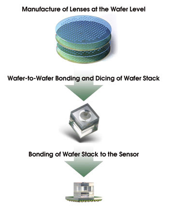
The optical advantage is not that wafer fabrication changes the laws of imaging. Its primary opportunity is repeatable batch manufacture and alignment of small components. It can also help make very short, integrated modules. But the allowable decentration and tilt remain set by image quality, and manufacturing many units together couples their yields: a wafer-level error can affect an entire array. Replicable surfaces and materials must also meet the lens’s requirements for aberration correction, wavelength response, temperature stability, and flare.
Keep wafer-level optics distinct from the microlenses on pixels discussed earlier. A pixel microlens directs light already arriving at the sensor toward a photosensitive region. The camera’s imaging lens forms the scene image on that sensor. Both can be manufactured in arrays, but they solve different optical problems. Nor is wafer-level assembly a universal replacement for individually assembled multi-element smartphone lenses; the appropriate method depends on performance and manufacturing requirements.
Folded optics: using length inside a thin device
A conventional camera module usually points its optical axis through the device’s thickness. For a distant subject, thin-lens geometry places the image approximately one focal length behind the lens. A real multi-element lens has a more complicated relation between effective focal length and physical track length, but a longer focal length still creates a substantial packaging challenge in that orientation.
Field of view makes the motive clear. For a sensor dimension and effective focal length , the angular field along that dimension is approximately
For an illustrative sensor dimension, gives a field of view of about ; gives about . With the same sensor, the latter provides a much narrower optical view. Packing its required optical path straight through a thin chassis is difficult.
A folded lens path uses a prism or mirror to redirect light so that much of the path runs laterally within the device. It trades device footprint for thickness. The fold changes where the path fits, not the focal length, field of view, or photon requirement.
In particular, at f-number , the entrance-pupil diameter is . If the illustrative lens operates at , it needs a entrance pupil. Folding a long path does not make that opening disappear. Aperture size, sensor dimensions and orientation, prism size, alignment, and available lateral space can all become limiting. Extra optical interfaces can also introduce losses and flare. A folded module is thus an effective way to package a longer-focal-length camera, not a general escape from optical size constraints.
One space budget, four different interventions
These techniques are easiest to evaluate by asking which constraint each one moves:
| Intervention | Constraint it addresses most directly | Constraint it does not remove |
|---|---|---|
| Backside illumination | Obstructed light path into small pixels | Photon count set by incident light and pixel area |
| Stacked sensor | Planar area and process competition between sensing and circuitry | Optical aperture and potential interconnect penalties |
| Wafer-scale optics | Repeated assembly and alignment of miniature optical units | Aberration tolerances and manufacturing yield |
| Folded lens path | Optical path length through device thickness | Required pupil size and physical module volume |
The approaches can be complementary: a folded lens may feed a BSI stacked sensor, while wafer-level methods may suit parts of its optical or packaging design. Their success, however, should be assessed by measurable outcomes—detected signal, crosstalk, noise, field of view, image quality, module dimensions, and manufacturability—rather than by whether the finished phone contains a particular technology.
Conclusion
Smartphone camera evolution is an exercise in redistributing physical constraints. BSI clears a better optical route into small pixels; stacking allocates sensing and electronics across layers; wafer-scale optics addresses miniature-assembly manufacture; and folded optics places a longer light path across the device rather than straight through it. None makes aperture, photon statistics, alignment, or heat irrelevant.
The next lesson examines what happens when hardware alone cannot supply the desired result: burst fusion, computational HDR, synthetic depth of field, and multi-frame super-resolution use multiple measurements and computation to make different trade-offs with optical and sensor hardware.