Recommended resources
The freely available resources this lesson will direct you to.
Hello. Last lesson established how photons become stored electrons and why quantum efficiency, full-well capacity, and conversion gain describe different limits. A CCD adds a distinctive engineering step: instead of measuring each pixel’s charge where it was collected, it moves charge packets across the chip to a shared output. Understanding that journey explains both the CCD’s architecture and its demanding transfer-efficiency requirements.
This lesson follows one packet from exposure to voltage readout. Allow about 40–45 minutes, including the readings.
A pixel as a place to store charge
In a CCD, as in the sensors discussed last lesson, an absorbed photon can generate an electron–hole pair. The useful electron must be collected and retained during the exposure. The CCD’s defining idea is to make that storage location movable: voltages on insulated electrodes shape the electric potential in silicon, confining electrons first under one set of electrodes and then under the next.
George E. Smith’s Nobel lecture gives an account of the original device concept. Read its MOS-capacitor explanation alongside Figures 3–6. The later passages on buried channels and area imagers show how a working shift register became a practical image sensor.
[PDF] Nobel Lecture by George E. Smith
Read Smith’s account for the physical idea behind a CCD and the problems encountered when it was turned into an imager.
Around pp. 95–96, use Figures 3–6 to orient yourself. Start in the discussion beside Figure 3 at storing and shifting; continue through the end of that Figure 5 discussion. Beside Figure 6, read the shift register. Focus on what represents the signal: the charge packet, not a voltage passed along a wire. Around pp. 99–101, find Figures 10 and 11 and read the buried channel. Then, beside Figure 12, read the area imager. Notice why the storage region makes exposure and readout compatible.
The insulated electrode and the silicon beneath it form a MOS structure. An applied gate voltage changes the silicon’s electrostatic potential, creating a region where electrons can be confined. It is helpful to call this a potential well, provided the sign is kept straight: an electron’s potential energy is lower where the electrostatic potential is more positive. During integration, collected electrons accumulate in a well; the packet’s electron count represents the light received at its image location.
Smith’s first devices moved charge near the silicon–oxide interface. Defects at that interface could temporarily trap electrons and release them after the packet had moved on. In a buried-channel CCD, the transfer path is engineered beneath the surface, reducing exposure to those traps. This is a materials-and-device solution to a readout problem: making electrons is not enough if their packets cannot survive the trip to the output.
Moving a packet without losing its place
Imagine adjacent electrodes over a transfer channel. First, a gate holds a packet in its well. Raising the voltage on the neighbouring gate makes the destination favourable and allows the charge to spread toward it. Lowering the original gate then leaves the packet confined at the destination. Repeating appropriately timed voltage patterns—the clock phases—moves packets along the channel.
This is more precise than the usual “bucket brigade” analogy. No physical container travels, and a CCD does not hand a measured voltage from pixel to pixel. The electrodes reshape a continuous potential landscape so that electrons themselves move. Gates and channel geometry must also maintain boundaries between neighbouring packets; otherwise, adjacent pixel signals would mix.
Hamamatsu’s technical note gives a compact engineering treatment. Its two-phase example is worth comparing with Smith’s three-phase scheme: both move charge by clocking electrodes, but a two-phase register also needs a built-in potential asymmetry to set a preferred transfer direction.
[PDF] Technical note / CCD image sensors - Hamamatsu Photonics
Read the technical note by Hamamatsu Photonics to connect the original MOS-capacitor idea to CCD clocking terminology.
On the note’s printed p. 01, under “Structure, operating principle,” read potential wells, referring to Figure 1-1. Then go to printed p. 04, “Charge transfer operation 1 - 2,” and follow Figure 1-7 from the opening description of two electrodes per pixel through clock timing. Look for the note’s distinction between clock voltages and the device structure that establishes direction.
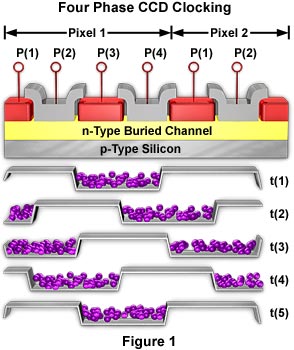
The Four Phase CCD Clocking image depicts four gates per repeating pixel structure rather than the note’s two-phase or Smith’s three-phase arrangement. The number of phases changes the clock implementation, not the governing principle: a sequence of neighbouring wells must offer each packet a controlled route forward. The drawn wells are a schematic of confinement, not a measured cross-section of electron potential energy.
Turning a two-dimensional exposure into a serial signal
A camera sensor needs one charge packet for each image location but does not need a separate output circuit at every location. In a CCD, many parallel (vertical) registers move packets toward a serial (horizontal) register. After a line of packets enters the horizontal register, it is clocked past the output one packet at a time. The vertical registers then supply the next line.
The exact route depends on where charge is accumulated:
- In a frame-transfer CCD, the illuminated image array itself acts as a parallel transfer register. After exposure, the frame is rapidly shifted into a light-shielded storage array. That stored frame is read line by line while the image array can collect the next exposure.
- In a full-frame CCD, the image area likewise holds and transfers charge, but there is no separate frame-storage array. An external shutter can prevent further illumination during readout.
- In an interline-transfer CCD, photodiodes collect charge beside shielded vertical registers. A transfer gate moves the collected packets into those registers before line-by-line readout.
These are different solutions to a timing problem, not different definitions of a CCD. The common feature is charge transport through clocked registers to an output.
For the complete path, read the frame-transfer and interline descriptions in Hamamatsu’s note, followed by its floating-diffusion output description.
[PDF] Technical note / CCD image sensors - Hamamatsu Photonics
Use the architecture and output sections of the same technical note to trace where a packet resides during exposure, transfer, and measurement.
On printed pp. 02–03, in “CCD types 1 - 1,” use Figure 1-2 and read the FT-type discussion beginning with its register layout. In particular, read from parallel to serial. In the “IT type” subsection, find “Two-dimensional type” beside Figure 1-5 and read photodiode transfer. Contrast where integration occurs in the two layouts. On printed p. 04, read “FDA 1 - 3” beside Figure 1-8, from output detection. Identify the sensing node, its reset operation, and why it can measure successive packets.

Follow one image location in the Frame-Transfer CCD Architecture image. Its packet begins in the illuminated array, enters the corresponding position in the storage array during the rapid frame shift, advances with its line into the bottom serial register, and is finally clocked to the output. Serial readout describes the output order; it does not mean that the scene was exposed one pixel at a time.
At the output, a common floating-diffusion node receives each packet. If its effective capacitance is and a packet contains electrons, the magnitude of the voltage change is approximately
where is the elementary charge. The node is reset before measuring the next packet. This is the conversion-gain relation from last lesson, now applied at a shared CCD output rather than used to describe a sensing node within each pixel. The resulting analogue voltage can subsequently be digitised. Sampling the reset and signal levels can suppress correlated reset-related noise, but it cannot undo charge lost or mixed during transfer.
Why transfer efficiency matters
Suppose each transfer delivers a fraction of a packet to the intended next well. In a simplified model with the same efficiency at every step, a packet of electrons undergoing transfers arrives with
Even gives : about two percent of the original charge would be missing from the intended packet after 2,000 transfers. Real trapping is more complicated than a constant fractional loss. Electrons released late can appear in following packets, producing trails around bright features rather than simply making every pixel slightly dimmer. That is why the buried-channel improvement in Smith’s account mattered so much.
Transfer also takes time. If an illuminated region continues generating charge while an exposed frame is being shifted, bright areas can leave smear along the transfer direction. A shutter, rapid frame transfer, shielding, or an interline layout can reduce this problem, with different costs in sensor area and complexity. These limitations arise from the same physical choice that makes the CCD elegant: the image is represented by mobile packets of charge until each reaches the output.
Conclusion
A CCD first collects photoelectrons in defined image locations. Clocked electrodes then reshape potential wells to transfer the packets through parallel and serial registers. At a shared output node, each packet becomes a voltage before digitisation. The architecture succeeds only if collection, confinement, timing, and transfer efficiency preserve the spatial pattern acquired during exposure.
Next, we will contrast this travelling-charge design with a CMOS active-pixel sensor, where amplification and addressing change how pixel signals reach the output.