Recommended resources
The freely available resources this lesson will direct you to.
Introduction
In our previous lesson, we explored how GPUs achieve high throughput by using a hardware-based warp scheduler to hide memory latency. We identified the Streaming Multiprocessor (SM) as the core computational engine where this scheduling and execution takes place. You learned that the SM manages a pool of resident warps, rapidly switching between them to keep its execution units busy.
This lesson directly addresses the learning outcome: Identify the key components of a modern GPU, such as Streaming Multiprocessors (SMs), and their roles. We will move from the abstract concept of the SM to a concrete architectural breakdown. Starting with a high-level view of the entire GPU die, we will progressively zoom in on its key functional blocks, culminating in a detailed examination of the SM itself. You will learn about the different types of processing cores, the on-chip memory structures, and the high-level components that orchestrate the entire system. This anatomical study is fundamental to understanding how a GPU's design is optimized for the massive parallelism required by AI workloads.
The Hierarchical Architecture of a GPU
Modern GPUs are not monolithic processors. Instead, they are organized hierarchically to manage the complexity of scheduling and executing tens of thousands of threads simultaneously. Think of it as a system of nested components, each responsible for managing a subset of the total workload.
Let's begin with a top-down view of a complete GPU die.
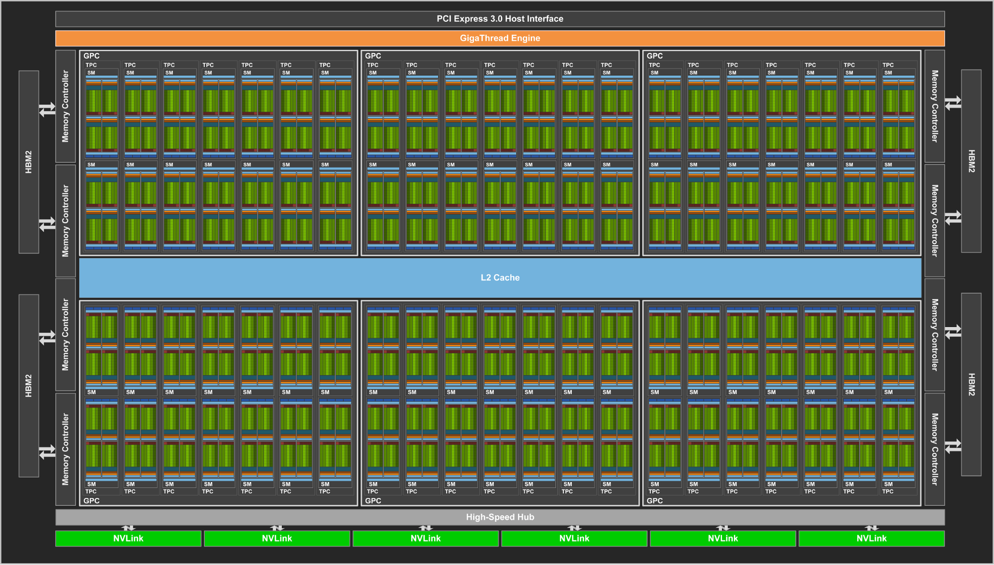
The key levels of this hierarchy are:
- The Full Chip: The entire silicon die, which includes all the processing units, memory controllers, and I/O interfaces.
- Graphics Processing Clusters (GPCs): The chip is partitioned into several GPCs. A GPC is a large, self-contained processing block that receives a portion of the total workload from a global scheduler.
- Streaming Multiprocessors (SMs): Each GPC contains multiple SMs. The SM is the true workhorse of the GPU. It is where thread blocks are assigned, scheduled, and executed. We will spend most of this lesson dissecting the SM.
There's a master hardware scheduler on the GPU that dispatches work to this hierarchy.
Inside the GPU: Hierarchical Compute Blocks
The following article provides a clear description of this hierarchical structure and introduces the master scheduler, called the 'Gigathread Engine' in NVIDIA's terminology.
Please read two short sections from the article 'Inside the GPU: A Guide to Modern Graphics Architecture'. First, read the section 'Hierarchical Compute Blocks' to see the GPC-to-SM breakdown. Then, jump down to the 'SIMT (Single Instruction, Multiple Threads)' section and read the description of the 'Gigathread Engine' to understand its role as the global hardware scheduler.
This hierarchical design allows the GPU to partition a massive compute problem (like a kernel launch with millions of threads) into manageable chunks that are distributed across the GPCs and ultimately assigned to individual SMs for execution.
Inside the Streaming Multiprocessor (SM)
Now, let's zoom into the most important component: the Streaming Multiprocessor. All the concepts we've discussed—threads, warps, scheduling, and latency hiding—come to life inside the SM. An SM is a highly parallel, self-contained processor with its own instruction pipeline, execution units, and memory.
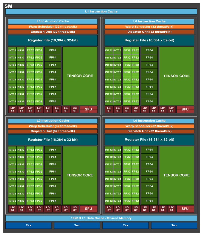
As the diagram shows, an SM is composed of several key sub-components. Let's examine their roles, especially in the context of your goal to understand AI system design.
To ground this discussion, we'll refer to the architecture of the NVIDIA A100 GPU, a datacenter workhorse designed for AI and HPC.
[PDF] NVIDIA A100 Tensor Core GPU Architecture
The NVIDIA A100 whitepaper provides an authoritative look at a modern SM. Please read the following sections to get an overview and see the official diagrams.
Read the sections 'NVIDIA A100 Tensor Core GPU Architecture In-Depth' (page 19) and 'A100 SM Architecture' (pages 20-22). Focus on Figure 6, which shows the full GPU, and Figure 7, which shows the detailed SM diagram. The text provides a summary of the SM's key features.
Drawing from the diagrams and text you just reviewed, let's break down the SM's main functional units:
1. Processing Cores
These are the units that perform the actual calculations.
- CUDA Cores (FP32/INT32 ALUs): These are the fundamental arithmetic logic units (ALUs) of the SM. They handle standard floating-point (FP32) and integer (INT32) operations. When a warp is scheduled, its instruction (e.g.,
c = a + b) is executed across a set of these cores for all 32 threads. - Tensor Cores: These are highly specialized processing units designed to accelerate one specific operation: the matrix multiply-accumulate (MMA), i.e., . This operation is the computational backbone of deep learning, forming the basis of both dense layers and convolutions. Tensor Cores can perform this MMA operation on small matrices (e.g., 4x4 or 8x8) with mixed precision (e.g., using FP16 inputs and FP32 accumulators) far more efficiently than general-purpose CUDA cores. For AI workloads, the performance of the Tensor Cores is often the most critical factor.
[PDF] NVIDIA A100 Tensor Core GPU Architecture
Let's dive deeper into Tensor Cores. Their introduction was a pivotal moment in GPU architecture for AI. This section of the A100 whitepaper explains their function and impact on performance.
Read the section 'Third-Generation NVIDIA Tensor Core' (pages 23-27). Pay attention to the explanation of the MMA operation and the various data types supported, like TF32, which was designed to accelerate standard FP32 AI code with minimal effort.
- Other Specialized Units (SFU, RT Cores): GPUs also contain Special Function Units (SFUs) for transcendental operations (e.g.,
sin,cos,sqrt) and, in consumer GPUs, RT Cores for ray tracing. While important, they are less central to the deep learning workloads you are focused on.
2. Memory Subsystem
Each SM has its own local, high-speed memory hierarchy to feed its powerful cores.
- Register File: A large bank of registers that hold the private state for each thread (e.g., local variables). The context for all resident warps (registers for 32 threads per warp) is stored here, enabling the zero-cost context switching we discussed previously.
- L1 Cache / Shared Memory: A small, extremely fast on-chip SRAM that serves a dual purpose. It can be configured as a hardware-managed L1 data cache and/or a software-managed shared memory. As shared memory, it can be used by threads within the same thread block to explicitly share data and cooperate, drastically reducing the need to go to the much slower global memory. We will explore this in detail in Module 3.
3. Control Logic
- Warp Schedulers and Dispatch Units: As covered in the last lesson, these hardware units select a ready warp from the pool of resident warps on every clock cycle and dispatch its next instruction to the appropriate execution units (CUDA Cores, Tensor Cores, etc.). The A100 SM diagram shows one warp scheduler per SM partition.
The Full Picture: GPU-Level Components
Now, let's zoom back out to the full chip level to see the components that support all the SMs.
- L2 Cache: A large, unified cache that is shared by all SMs on the GPU. It acts as a backstop for the SMs' L1 caches, capturing data that is shared across different thread blocks or is too large to fit in L1. A larger L2 cache can significantly improve performance by reducing traffic to the main memory.
- High-Bandwidth Memory (HBM) / GDDR: This is the GPU's main off-chip DRAM, often referred to as global memory in CUDA. It has enormous bandwidth (e.g., >1.5 TB/s on A100) but also much higher latency compared to on-chip caches. The primary challenge in GPU programming is structuring computation to keep the SMs fed from this memory.
- Interconnects (PCIe, NVLink): These are the data links that connect the GPU to the rest of the system.
- PCI Express (PCIe) is the standard interface connecting the GPU to the CPU's motherboard.
- NVLink is a proprietary, high-speed interconnect from NVIDIA that connects multiple GPUs directly to each other, offering much higher bandwidth than going through the CPU via PCIe. This is critical for scaling large model training across multiple GPUs.
The following video provides a more dynamic explanation of how these pieces fit together, focusing on how a thread block is mapped onto an SM and consumes its resources.
Stanford CS149 I Parallel Computing I 2023 I Lecture 7 - GPU architecture and CUDA Programming
This lecture segment walks through the architecture of an SM and explains how a Cuda thread block is scheduled onto it, allocating the necessary execution contexts and shared memory.
Watch from 50:02 to 1:12:15. The speaker builds up an SM from its components (ALUs, execution contexts, shared memory) and then demonstrates how the GPU's scheduler assigns thread blocks to the SMs based on their resource requirements. This is a crucial link between the software programming model and the hardware reality.
Conclusion
In this lesson, we dissected the architecture of a modern GPU, identifying its key components and their functions. We adopted a top-down approach, starting from the full chip and zooming into the all-important Streaming Multiprocessor.
Key Takeaways:
- Hierarchical Design: GPUs are organized into Graphics Processing Clusters (GPCs), which contain multiple Streaming Multiprocessors (SMs). A global scheduler (Gigathread Engine) distributes work across this hierarchy.
- The Streaming Multiprocessor (SM): The core execution engine of the GPU where thread blocks run. It is a processor-on-a-chip containing:
- CUDA Cores: General-purpose ALUs for FP32 and INT32 math.
- Tensor Cores: Specialized accelerators for matrix-multiply-accumulate (MMA) operations, which are fundamental to deep learning performance.
- On-chip Memory: A large Register File for thread-private state and a combined L1 Cache/Shared Memory for fast data access and inter-thread cooperation within a block.
- Control Logic: Warp Schedulers that orchestrate execution by hiding latency.
- GPU-Level Components: The SMs are supported by a large shared L2 Cache, high-bandwidth off-chip memory (HBM/GDDR), and interconnects like PCIe and NVLink.
Preview of the Next Lesson:
We have now identified the key components of the GPU, especially its compute units (SMs) and various memory spaces (registers, shared memory, L1/L2, HBM). In the next module, "GPU Memory Hierarchy and Data Movement," we will focus specifically on this memory system. Our first lesson will be to diagram the GPU memory hierarchy, analyzing the characteristics (size, bandwidth, latency) of each level and beginning to understand how data movement between them dictates application performance.