Recommended resources
The freely available resources this lesson will direct you to.
Hello! This course begins with the skill that makes the later building and measuring possible: reading a circuit diagram. For this lesson, the goal is not to calculate how much a pedal boosts a signal. It is to look at a simple booster schematic and reliably answer three questions: What is each symbol? Which terminals are electrically connected? Where does the guitar signal enter and leave?
A schematic is a map of electrical relationships, not a picture of where parts sit inside a pedal. Once you can read that map, a unfamiliar circuit becomes much easier to investigate.
Learn the symbols you need first
Start with the short demonstration below. Watch for the difference between a component’s symbol (what kind of part it is), its designator (which particular part it is), and its value (a property or part number).
Introduction to reading an electronic schematic
Watch “Introduction to reading an electronic schematic” from DIY Guitar Pedals for a visual introduction to the parts that appear repeatedly in pedals.
Watch capacitors and resistors for their symbols, labels, and the polarity mark on an electrolytic capacitor. Then watch the potentiometer: the arrow is its movable contact, called the wiper, and is a third electrical terminal.
The reference chart below contains far more symbols than you need today. Concentrate on its resistors, variable resistors, capacitors, batteries, voltage nodes, and BJTs. The other rows will become useful as the course reaches other pedal circuits.
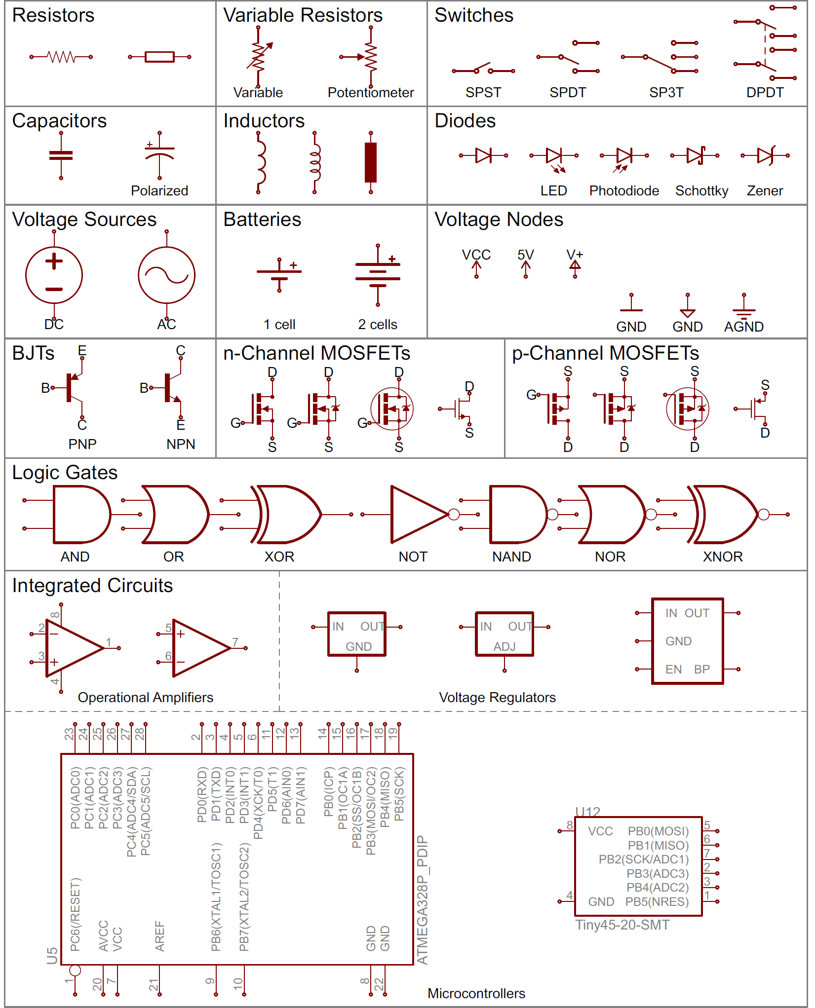
A resistor may be drawn as a zigzag or a rectangle; neither drawing specifies its physical appearance. A capacitor has two terminals, depicted by plates. If a capacitor symbol has a curved plate or a marked positive side, polarity matters. A potentiometer has two ends of a resistive element and a wiper, so it must not be mistaken for an ordinary two-terminal resistor.
Read the selected portions of SparkFun’s How to Read a Schematic as a compact symbol reference. You do not need to study its sections on inductors, logic gates, or microcontrollers yet.
SparkFun’s guide puts the symbols alongside the names and values used to identify individual parts. Read it to make the reference chart usable when you encounter a real pedal schematic.
In “Schematic Symbols (Part 1),” read the “Resistors,” “Potentiometers and Variable Resistors,” and “Capacitors” subsections, from resistors through capacitors. Later in that same section, inspect “Batteries” and “Voltage Nodes.” In “Schematic Symbols (Part 2),” read only “Bipolar Junction Transistors (BJTs),” from the BJT description to the NPN identification. Finally, in “Name Designators and Values,” read from names and values; focus on why a label such as R1 identifies a particular resistor rather than describing its electrical value.
You will often see R for resistor, C for capacitor, and Q for transistor. Thus, “R1 430K” identifies one particular resistor and gives its resistance; “C1 100nF” identifies one capacitor and gives its capacitance. These labels are useful precisely because a circuit can contain several identical-looking symbols with different connections or values. A transistor’s terminal names matter too: the NPN transistor in our example has a base, collector, and emitter. The schematic tells you which role each terminal plays; the shape of a real transistor package alone does not guarantee which physical lead is which.
Connections matter more than proximity
Imagine highlighting a continuous wire on a schematic. Every component terminal reached without passing through a component belongs to the same net: an electrically connected set of points. A junction dot marks a connection where lines meet. Conversely, when two lines merely cross without a junction dot, the convention used in the guide is that they do not connect. If a drawing is unclear, do not silently assume a connection; check its junction marks and labels.
The diagram may also avoid drawing a long wire by giving separated nets the same name. Every occurrence of a ground symbol labeled GND, for example, denotes the same ground net, even if those symbols are scattered around the page. Ground is a shared electrical reference and return connection—not an instruction to place every grounded part at the bottom of a physical build.
Continue SparkFun’s guide for the conventions that decide whether two terminals are connected. These conventions are more important than how close the symbols appear on the page.
Under “Nets, Nodes and Labels,” read “Junctions and Nodes” and “Net Names,” from nets through labels. Compare its connected and unconnected crossing illustrations. Then, under “Schematic Reading Tips,” read “Identify Blocks” and “Recognize Voltage Nodes,” from blocks and voltage nodes. Notice that blocks organize the drawing, while voltage-node symbols specify connections.
A useful distinction is same net versus connected through a part. The two terminals of a resistor are generally not the same node; the resistor sits between two nodes. The same is true of a capacitor. This distinction prevents a common reading error: a line that reaches one side of a component has not automatically reached the other side.
Schematics frequently arrange audio input toward the left, audio output toward the right, supply near the top, and ground near the bottom. Treat that as a reading convention, not an electrical rule. Branches toward power or ground still matter even when the main audio path appears to run straight across the page.
Read a booster pedal as connected blocks
Here is an annotated schematic of a simple LPB-1-style guitar booster. Its colored rectangles identify functional blocks for the reader; their borders are not wires. Follow the drawn wires, junction dots, component terminals, and GND symbols instead.

Begin at J1 IN. Its contact marked T is the input signal connection. The contact marked S goes to GND. Guitar-pedal schematics sometimes abbreviate jacks to a single input or output wire; the missing-looking connection is usually the cable’s grounded sleeve. The short reading below explains that convention without requiring you to learn jack wiring in detail yet.
Read the “Inputs and Outputs” explanation in From Schematic to Reality to connect a schematic’s signal line and ground reference to a guitar cable.
In “Inputs and Outputs,” begin just below Figure 2.2 at the paragraph about the plug’s tip and sleeve. Read jack shorthand, stopping after the comparison with Figure 2.3. Focus on why an input shown as one signal wire still needs a ground connection.
Now trace the booster, separating the audio route from connections that support the transistor:
- From J1’s T contact, the incoming signal reaches the left terminal of C1, marked 100nF. Its right terminal reaches a junction dot. That dot connects the right side of C1, the lower end of R1, the upper end of R3, and the base of Q1. They all meet at one node. The signal does not have to travel “through R1 and then R3” to reach the base: those resistors are branches from the base node.
- Q1 is the transistor in the gain block. Its collector connects to the lower end of R2 and the left side of C2. Its emitter connects through R4 to GND. The guitar’s variation at the base affects the transistor’s behavior at its collector; there is no ordinary wire directly joining base to collector. You can recognize that signal relationship now without calculating transistor gain.
- From the collector node, the outgoing audio reaches C2 and then the upper end of RV1, the volume potentiometer. RV1’s lower end goes to GND. Its wiper, shown by the arrow and marked terminal 2, connects to J2’s T contact. J2’s S contact goes to GND. Changing the wiper position changes the level delivered to the output.
The 9 V battery, BT1, supplies a different essential part of the picture. Its positive terminal connects to the upper ends of R1 and R2; its negative terminal connects to GND. R3 and R4 also end at GND. The repeated ground symbols therefore stand for shared connections, not several unrelated grounds. R1 through R4 help establish conditions for Q1 to operate, while C1 and C2 sit at the boundaries of the gain stage. We will distinguish steady supply voltages from changing audio voltages—and calculate what the resistors do—in upcoming lessons.
Notice how much you can already say without doing those calculations. You can locate the input and output, list everything attached to the base and collector nodes, identify the supply connections, and find the terminal that actually delivers the volume-controlled output. You can also avoid two tempting mistakes: interpreting the colored annotation boxes as conductive traces, or assuming the transistor’s three drawn terminals reveal its physical lead order. A schematic specifies electrical roles; a particular part’s pinout must be checked separately when it is time to build.
A reliable way to approach the next schematic
When a new pedal drawing looks crowded, first identify its input, output, supply, and ground. Next, recognize the component symbols and read their designators. Then trace one node at a time: stop at each component terminal, account for every dotted branch, and resume on the component’s other side only when following the circuit further. Finally, group the drawing into functions such as input, gain stage, and level control. This keeps the left-to-right audio story clear without overlooking the supply and ground branches that make it work.
You have now read a simple booster at the level needed for the first learning outcome: symbols tell you what each part is, nets tell you what connects, and functional blocks help you follow the guitar signal from jack to jack. Next, you will use voltage, current, resistance, and basic circuit laws to put numbers to some of the relationships this schematic shows.