In our previous lesson, we established a foundational model of the CPU, identifying the Arithmetic Logic Unit, Control Unit, and registers as its core components. We ended with the understanding that these parts work in a coordinated, cyclical process—the Fetch-Decode-Execute cycle—to run programs. Now, we will dissect that cycle piece by piece.
Our goal today is to describe exactly how an instruction is fetched from memory, interpreted by the Control Unit, and finally carried out by the hardware. We will move beyond a high-level overview and trace the precise flow of information through the CPU for each stage. This level of detail is crucial for understanding how software, including the OS you will build, directs the physical machinery of the computer.
A More Detailed Model and a New Language
To trace an instruction's journey, we need to introduce a few more specialized registers that act as intermediaries between the CPU and main memory (RAM). Your background in electronics will make the concept of dedicated registers for specific interfacing tasks feel quite natural.

The key new registers are:
- Memory Address Register (MAR): This register holds the memory address that the CPU wants to read from or write to. It is the CPU's sole gateway to the address bus.
- Memory Data Register (MDR) (also called Memory Buffer Register, MBR): This register temporarily holds the data that has just been read from memory or is about to be written to memory. It is the gateway to and from the data bus.
To describe the operations within the CPU, we will use a notation called Register Transfer Language (RTL). RTL is a simple way of expressing the transfer of data between registers. For example, to say "the contents of the Program Counter are copied into the Memory Address Register," we write:
MAR ← PC
Each RTL statement corresponds to a micro-operation, a fundamental action that the Control Unit orchestrates by sending electrical signals to open and close pathways between components.
The following lecture notes introduce a "Bog Standard Architecture" that formalizes this model. It's an excellent resource for understanding the roles of these specific registers.
Lecture 2 The CPU, Instruction Fetch & Execute
These notes from the University of Oxford provide a clear, structured view of a classic CPU architecture.
Please read the introduction and the section A Bog Standard Architecture (pages 1-4). Focus on the descriptions of the CPU registers, especially the MAR, MBR, PC, IR, and AC (Accumulator). This will solidify the roles of the components we'll be tracking. Don't worry about the register widths (e.g., 24-bit vs 16-bit) for now; focus on their functions.
Phase 1: The Fetch Stage
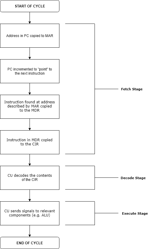
The cycle begins with fetching the next instruction from memory. This process is the same for every instruction, regardless of what it does. The CPU must first retrieve the instruction before it can know what to do. The Program Counter (PC) always holds the address of this next instruction.
The fetch operation consists of a precise sequence of micro-operations:
MAR ← PC: The address of the next instruction is copied from the Program Counter to the Memory Address Register. The CPU is now prepared to tell memory which location it's interested in.MBR ← ⟨MAR⟩: The CPU places the address from the MAR onto the address bus. The Control Unit then sends a "read" signal to memory. Memory responds by placing the contents of the specified location onto the data bus, which is then loaded into the Memory Buffer Register. The notation⟨MAR⟩means "the contents of the memory location pointed to by MAR."IR ← MBR: The instruction that was fetched into the MBR is now moved to the Instruction Register (IR). The CPU is now ready to figure out what the instruction means.PC ← PC + 1: While the current instruction is being processed, the Program Counter is incremented to point to the address of the next instruction in the sequence. This prepares the CPU for the next fetch cycle.
These steps are universal. The CPU blindly fetches whatever is at the address in the PC, increments the PC, and assumes it's an instruction.
Let's refer back to the lecture notes for a formal description of this sequence.
Lecture 2 The CPU, Instruction Fetch & Execute
This section formalizes the fetch process using RTL.
Read the sections titled The Fetch, Decode, Execute Cycle and Fetching and decoding an instruction. Note how the RTL lines directly correspond to the steps described above.
This sequence of fetching an instruction is a fundamental rhythm of the CPU, driven by the system clock. The video below provides an excellent animation of this process.
The Fetch Decode Execute Cycle
This video from Computer Science Lessons provides a clear visualization of the data flow between the CPU and RAM.
First, watch the overview of the components from the start of the visualization to understand the setup. Then, pay close attention to the fetch stage animation from this segment. Observe how the PC's value moves to the MAR, an instruction is retrieved from RAM into the MDR (MBR), and finally into the CIR (IR), followed by the PC incrementing.
Phase 2: The Decode Stage
Now that the instruction is in the Instruction Register (IR), the Control Unit (CU) takes over. The instruction, which is just a binary number, is typically divided into two parts:
- Opcode (Operation Code): Specifies the operation to be performed (e.g., load, add, store).
- Operand(s): Specifies the data or memory location to be used for the operation.
The CU has built-in decoder circuitry that interprets the opcode. Based on this opcode, the CU generates the specific sequence of control signals needed for the execute stage. Think of the CU as a finite state machine where the inputs are the opcode and the current step in the execution, and the outputs are the control signals that enable or disable every other component.
The "8-bit CPU control logic" video by Ben Eater offers an exceptionally clear look at this process. He conceptualizes the entire control logic as a lookup table implemented in EEPROMs, which should resonate with your electronics background.
8-bit CPU control logic: Part 3
This video gets into the weeds of implementing control logic. It shows how the combination of the current instruction and the current step in the cycle determines which control signals are active.
Watch from the beginning to where he explains the fetch steps. Focus on the two key inputs to the control logic: the instruction in the IR and the current time step (T0, T1, etc.). He demonstrates that for steps T0 and T1 (the fetch stage), the control signals are the same regardless of the instruction.
Phase 3: The Execute Stage
This is where things get interesting, because the actions performed in this stage depend entirely on the instruction that was decoded. Let's look at a few examples using the architecture from our lecture notes.
Example 1: LDA x (Load Accumulator from memory address x)
The goal is to load a value from a memory location x into a general-purpose register called the Accumulator (AC).
The decoded opcode for LDA triggers the following micro-operations:
MAR ← IR(address): The operand part of the instruction (the addressx) is copied from the IR to the MAR.MBR ← ⟨MAR⟩: The CPU fetches the data from addressxinto the MBR.AC ← MBR: The data is finally copied from the MBR into the Accumulator. The instruction is now complete.
Example 2: ADD x (Add contents of memory address x to Accumulator)
The goal is to add a value from memory to the value already in the Accumulator and store the result back in the Accumulator.
MAR ← IR(address): Same asLDA, the operand addressxis sent to the MAR.MBR ← ⟨MAR⟩: The data at addressxis fetched into the MBR.AC ← AC + MBR: The Control Unit directs the contents of the Accumulator and the MBR to the inputs of the ALU. It also sends a signal to the ALU telling it to perform an addition. The result from the ALU is then written back into the Accumulator, overwriting its previous value.
Notice how the sequence of micro-operations changes based on the instruction. The "Lecture 2" PDF and the "Fetch Decode Execute Cycle" video both walk through these specific examples.
Lecture 2 The CPU, Instruction Fetch & Execute
This section details the execute phase for several common instructions.
Read the section Executing an instruction. Follow the RTL steps for LDA x, STA x (Store Accumulator), and ADD x. Compare the sequence for LDA with ADD to see how the involvement of the ALU changes the final step.
Now, watch the visualization of these execute steps.
The Fetch Decode Execute Cycle
This video animates the execution of the exact instructions we just discussed.
Watch the execution of the LDA instruction from this segment, followed by the ADD instruction from the next segment, and finally the STA (store) instruction from this part. Try to match the animated data flow with the RTL steps you just read.
Conclusion
In this lesson, we have moved from a static picture of the CPU to a dynamic one, detailing the precise sequence of events that brings a program to life.
- The Fetch-Decode-Execute Cycle is the fundamental operation of the CPU, where each stage is comprised of smaller micro-operations.
- We use Register Transfer Language (RTL) to describe these micro-operations, which represent data moving between registers like the PC, MAR, MBR, and IR.
- The Fetch stage is universal:
MAR ← PC,MBR ← ⟨MAR⟩,IR ← MBR,PC ← PC + 1. - The Decode stage is where the Control Unit interprets the instruction's opcode, determining the subsequent steps.
- The Execute stage is instruction-specific, involving data transfers and potential calculations by the ALU, as we saw with the
LDAandADDexamples.
We have seen that the CPU is constantly reading from and writing to main memory. However, accessing memory is significantly slower than operations within the CPU itself. In our next lesson, we will explore the memory hierarchy—registers, caches, RAM, and storage—and understand why the differences in their speed and size are critically important for computer performance and OS design.