Welcome to your first lesson! I'm excited to guide you on your journey to understanding electronics, starting from the fundamental science that makes it all possible.
Your goal is to gain a deep, intuitive knowledge of how electronics work, right down to the physics of the components in your Arduino kit. This course is designed to do just that, building your understanding from the ground up.
In this first lesson, we will address the learning outcome: Explain the atomic structure of conductors, insulators, and semiconductors in terms of electron behavior.
We'll explore why copper carries electricity so well, why the plastic coating on wires stops it, and what makes silicon—the heart of your Arduino's microcontroller—so special. To do this, we'll touch on some core concepts from physics, connecting the behavior of single atoms to the properties of solid materials. This foundation is the first and most crucial step toward understanding every electronic component you'll encounter.
1. From Atoms to Energy Bands
At the heart of any material are atoms, composed of a nucleus and orbiting electrons. In your physics studies, you may have encountered the Bohr model, where electrons occupy discrete, specific energy levels or "shells" around an atom. An electron can't exist between these levels; it must jump from one to another by gaining or losing a precise amount of energy.
This picture changes when billions of atoms come together to form a solid crystal, like in a piece of copper or silicon. The strict energy levels of individual atoms are forced to merge and split, creating vast, continuous ranges of allowed energies called energy bands.
To understand this transformation, which is a quantum mechanical phenomenon, I'd like you to watch the following video. It provides an excellent, in-depth explanation starting from the behavior of a single electron and building up to the concept of energy bands in a solid. Given your interest in physics, you should find the derivation quite satisfying.
The Actual Reason Semiconductors Are Different From Conductors and Insulators.
This video, 'The Actual Reason Semiconductors Are Different From Conductors and Insulators,' explains how the quantum properties of electrons lead to the formation of energy bands. It's a detailed and foundational look at the physics.
Please watch the following two segments: Quantum Properties of Electrons (from 03:21 to 12:30): This part explains the fundamental quantum rules governing electron behavior, such as wave-particle duality and the Pauli exclusion principle. Focus on why electrons are restricted to specific energy states. From Atoms to Bonds to Bands (from 16:07 to 26:20): This is the core segment. It shows how the energy levels of individual atoms split and form continuous bands when they bond together in a solid. Pay close attention to the explanation of molecular orbital theory and how it resolves the 'capacity problem'.
To summarize the key ideas from the video:
- Discrete Levels to Bands: In an isolated atom, electrons occupy discrete energy levels. In a solid, these levels interact and smear out into wide energy bands, each containing a massive number of closely packed energy states.
- Pauli Exclusion Principle: This principle, which states that no two electrons can occupy the same quantum state, is the fundamental reason why energy levels split. When atoms get close, their electron orbitals overlap, and to avoid violating the principle, the original energy levels must split into new, distinct levels (bonding and anti-bonding orbitals), which ultimately form the bands.
- Filling the Bands: Electrons in a solid fill these energy bands starting from the lowest energies first, just as they would with atomic shells.
2. The Big Three: Conductors, Insulators, and Semiconductors
The electrical properties of any solid material are determined by two main factors:
- How its outermost energy bands are filled with electrons.
- The energy gap, if any, between these bands.
The two most important bands are:
- Valence Band (): The highest energy band that is completely full of electrons at absolute zero temperature. These electrons are typically involved in bonding atoms together and are not free to move.
- Conduction Band (): The next higher energy band, which is empty at absolute zero. If an electron can get into this band, it is free to move throughout the material and conduct electricity.
- Band Gap (): The energy difference between the top of the valence band and the bottom of the conduction band (). Electrons cannot exist within this "forbidden" energy gap.
The size of this band gap is what fundamentally distinguishes conductors, insulators, and semiconductors.
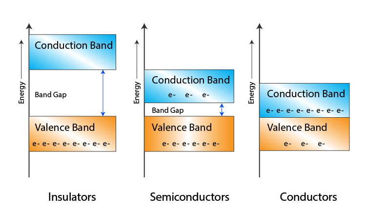
Let's break down each type:
Conductors (e.g., Copper, Aluminum)
- Band Structure: The valence band and conduction band overlap. There is no energy gap ().
- Electron Behavior: Since the bands overlap, electrons in the valence band are already in the conduction band. They require only a tiny amount of energy (from an applied voltage, for instance) to move into empty states and travel through the material. This results in a large flow of current.
Insulators (e.g., Glass, Rubber, Plastic)
- Band Structure: The valence band is completely full, the conduction band is empty, and they are separated by a large band gap (typically eV).
- Electron Behavior: An enormous amount of energy is required to excite an electron from the full valence band across the large gap into the empty conduction band. Under normal conditions, this doesn't happen, so there are no mobile electrons to carry current. This is why they don't conduct electricity.
Semiconductors (e.g., Silicon, Germanium)
- Band Structure: Similar to an insulator, but with a small, 'just right' band gap (for silicon, eV).
- Electron Behavior: At absolute zero, a semiconductor acts like an insulator. However, at room temperature, the thermal energy of the system is sufficient to "kick" a small number of electrons from the valence band across the small gap into the conduction band. These few electrons can now conduct electricity. This unique property—having conductivity that is sensitive to energy input like heat, light, or voltage—is what makes semiconductors the foundation of all modern electronics.
To reinforce these ideas with a helpful analogy, watch this short segment from another video.
Band theory (semiconductors) explained
The video 'Band theory (semiconductors) explained' provides a clear, concise summary and a great physical analogy to help you intuitively grasp these concepts.
Please watch the segment from 04:32 to 10:57. It first explicitly compares the band diagrams of the three material types and then uses an analogy with marbles on a dimpled surface to visualize how electrons behave in each case.
Now, let's turn to a more formal, textbook explanation to solidify your understanding of these distinctions.
Electrons and Holes in Semiconductors
This excerpt from the textbook 'Electrons and Holes in Semiconductors' provides a formal definition and comparison of the three material types based on their energy band diagrams.
Please read Section 1.4, titled 'Semiconductors, Insulators, and Conductors.' This is a short but precise section that summarizes the key differences we've just discussed.
Test your understanding!
Imagine you have three unknown materials. You measure the energy required to move an electron into the conduction band for each:
- Material A: 0.7 eV
- Material B: 8.0 eV
- Material C: 0.01 eV
How would you classify each material and why?
Show answer
- Material A is a semiconductor. Its band gap (0.7 eV) is small enough that thermal energy at room temperature can excite some electrons into the conduction band, allowing for moderate conductivity.
- Material B is an insulator. Its band gap (8.0 eV) is very large, making it practically impossible for electrons to jump into the conduction band under normal conditions.
- Material C is a conductor. The energy required is nearly zero (0.01 eV), which implies its valence and conduction bands are overlapping. Electrons are already free to move and conduct electricity.
3. The Bond Model and "Holes"
While the energy band model is the most accurate physical description, there is a simpler, more intuitive model for semiconductors like silicon called the bond model.
Silicon is in Group IV of the periodic table, meaning it has four valence electrons. In a silicon crystal, each atom forms a covalent bond with four neighboring atoms, sharing electrons so that each atom effectively has a full shell of eight electrons. At low temperatures, all electrons are locked in these bonds.
Electrons and Holes in Semiconductors
To visualize this, let's look again at the textbook 'Electrons and Holes in Semiconductors'. This section introduces the bond model, which is a very useful way to think about electron behavior in silicon.
Please read Section 1.2, 'Bond Model of Electrons and Holes'. Focus on Figure 1-4, which shows the covalent bonds, and Figure 1-5, which illustrates the creation of an electron-hole pair. The text also introduces the critical concept of a 'hole'.
As the reading explains, when an electron in a semiconductor gains enough thermal energy to jump to the conduction band, it breaks free from its covalent bond. This creates two things:
- A free electron in the conduction band, which can carry current.
- A hole: a vacancy left behind in the covalent bond.
This hole is a crucial concept. A neighboring electron can easily move into this hole, effectively causing the hole to move in the opposite direction. It's much simpler to think of this as a mobile positive charge carrier moving through the crystal. In semiconductors, the current is carried by both the movement of negative electrons and the movement of these positive holes.
Conclusion
In this lesson, we established the fundamental scientific principles that govern electrical conductivity. You now have two models to understand this: the rigorous energy band model and the intuitive bond model.
Here are the key takeaways:
- Electrons in solids exist in energy bands due to quantum mechanical effects.
- The outermost important bands are the valence band (filled) and the conduction band (empty). They are separated by a band gap.
- Conductors have overlapping bands (), allowing electrons to move freely.
- Insulators have a very large band gap ( eV), preventing electron movement.
- Semiconductors have a small band gap ( eV). This allows a small, controllable number of electrons to enter the conduction band, leaving behind movable holes in the valence band.
This ability to precisely control conductivity is what makes semiconductors the key ingredient for all the components you'll be working with, from diodes to transistors to the complex microcontroller in your Arduino.
In our next lesson, we will move from the microscopic behavior of electrons to the macroscopic world of circuits. We'll start by defining electric charge and then use Coulomb's Law to calculate the force between charges, which is the driving force behind all electricity.