Introduction
Welcome back! In our last lesson, we identified the key components within the CPU—the Control Unit (CU), the Arithmetic Logic Unit (ALU), and registers—and conceptually outlined their roles in the Fetch-Decode-Execute cycle. You learned what each component does.
Today, we're going to put that knowledge into practice. Our learning outcome is to trace the fetch-decode-execute cycle for simple instructions. We will move from the "what" to the "how" by performing a step-by-step trace of a simple program. You will see exactly how the values in the registers and memory change as the CPU brings each instruction to life. This detailed perspective is fundamental to understanding how software actually runs on hardware.
Setting the Stage: A Simple Computer Model
To trace the cycle, we need a simplified model of a computer. Imagine a CPU connected to a small amount of RAM.
The CPU contains these key registers:
- Program Counter (PC): Holds the memory address of the next instruction.
- Memory Address Register (MAR): Holds the address of the memory location to be accessed.
- Memory Data Register (MDR): Temporarily holds data or instructions moving between the CPU and memory.
- Current Instruction Register (CIR): Holds the instruction currently being decoded and executed. (Also often called the Instruction Register, or IR).
- Accumulator (AC): A general-purpose register used by the ALU to hold data and the results of calculations.
The RAM contains our program and data:
Let's assume our program starts at memory address 10. The program's goal is to add two numbers (20 and 30) and store the result.
| Memory Address | Contents (Instruction / Data) | Description |
|---|---|---|
| ... | ... | ... |
| 3 | 20 | Data value |
| 4 | 30 | Data value |
| 5 | 0 | Memory location for the result |
| ... | ... | ... |
| 10 | LDA 3 |
Load data from address 3 into AC |
| 11 | ADD 4 |
Add data from address 4 to AC |
| 12 | STA 5 |
Store data from AC into address 5 |
| ... | ... | ... |
To describe the operations within the CPU, we'll use a notation called Register Transfer Language (RTL), which is a concise way to represent the movement of data. For example, MAR <- PC means "copy the contents of the Program Counter into the Memory Address Register."
Let's begin the trace. We'll assume the PC starts at 10, the address of our first instruction.
Tracing the Fetch-Decode-Execute Cycle
The following video provides a brilliant animation of this exact process. We will watch it in segments, pausing to analyze the state of our computer model at each step.
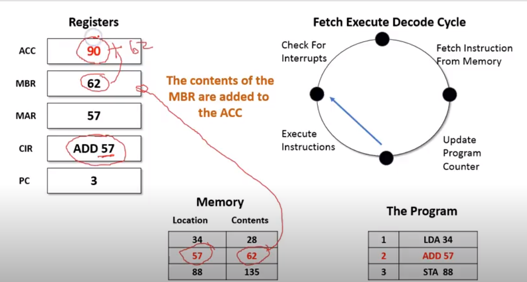
The Fetch Decode Execute Cycle
This video provides a detailed, animated walkthrough of the Fetch-Decode-Execute cycle using a simple program very similar to our example. It clearly visualizes the flow of data between the registers and memory.
You don't need to watch the whole video at once. I will guide you to specific timestamps as we trace each instruction. The video uses a slightly different starting address but the process is identical.
Instruction 1: LDA 3
The PC starts at 10. All other registers are empty.
1. Fetch Phase
The CPU needs to retrieve the instruction from memory address 10.
- Step 1: The address of the instruction is moved from the PC to the MAR.
- RTL:
MAR <- PC
- RTL:
- Step 2: The CPU reads from memory. The instruction at the address specified by the MAR is copied to the MDR.
- RTL:
MDR <- Memory[MAR]
- RTL:
- Step 3: The instruction is moved from the MDR to the CIR to be decoded. At the same time, the PC is incremented to point to the next instruction (
11).- RTL:
CIR <- MDR; PC <- PC + 1
- RTL:
State after Fetch:
| PC | MAR | MDR | CIR | AC |
|---|---|---|---|---|
| 11 | 10 | LDA 3 |
LDA 3 |
0 |
Now, watch the video from 07:57 to 10:04 to see this fetch phase animated.
2. Decode & Execute Phase
The Control Unit decodes the instruction LDA 3 in the CIR. It understands that it needs to load data from memory address 3.
- Step 4: The address part of the instruction (
3) is placed in the MAR.- RTL:
MAR <- CIR(address)
- RTL:
- Step 5: The CPU reads from memory again. The data at the address in the MAR is copied to the MDR.
- RTL:
MDR <- Memory[MAR]
- RTL:
- Step 6: The data is copied from the MDR into the Accumulator. The instruction is now complete.
- RTL:
AC <- MDR
- RTL:
Final State after Instruction 1:
| PC | MAR | MDR | CIR | AC |
|---|---|---|---|---|
| 11 | 3 | 20 | LDA 3 |
20 |
Watch the video from 10:04 to 11:22 to see the decode and execute phase for the
LDAinstruction.
Instruction 2: ADD 4
The cycle repeats for the next instruction. The PC is currently 11.
1. Fetch Phase
- RTL:
MAR <- PC(MAR becomes11) - RTL:
MDR <- Memory[MAR](MDR getsADD 4) - RTL:
CIR <- MDR; PC <- PC + 1(CIR getsADD 4, PC becomes12)
State after Fetch:
| PC | MAR | MDR | CIR | AC |
|---|---|---|---|---|
| 12 | 11 | ADD 4 |
ADD 4 |
20 |
2. Decode & Execute Phase
The CU decodes ADD 4. It knows it must add the contents of memory address 4 to the Accumulator. This requires the ALU.
- Step 4: The address part (
4) is placed in the MAR.- RTL:
MAR <- CIR(address)
- RTL:
- Step 5: The data at address
4is fetched into the MDR.- RTL:
MDR <- Memory[MAR]
- RTL:
- Step 6: The CU instructs the ALU to add the value in the AC to the value in the MDR, and store the result back in the AC.
- RTL:
AC <- AC + MDR
- RTL:
Final State after Instruction 2:
| PC | MAR | MDR | CIR | AC |
|---|---|---|---|---|
| 12 | 4 | 30 | ADD 4 |
50 |
Watch the video from 11:22 to 12:57 to see the full cycle for the
ADDinstruction, including the involvement of the ALU.
Instruction 3: STA 5
The PC is at 12. The AC holds the result, 50.
1. Fetch Phase
- RTL:
MAR <- PC(MAR becomes12) - RTL:
MDR <- Memory[MAR](MDR getsSTA 5) - RTL:
CIR <- MDR; PC <- PC + 1(CIR getsSTA 5, PC becomes13)
State after Fetch:
| PC | MAR | MDR | CIR | AC |
|---|---|---|---|---|
| 13 | 12 | STA 5 |
STA 5 |
50 |
2. Decode & Execute Phase
The CU decodes STA 5. This is a write operation. The goal is to copy the value from the AC into memory.
- Step 4: The address part (
5) is placed in the MAR.- RTL:
MAR <- CIR(address)
- RTL:
- Step 5: The data to be written (
50) is moved from the AC to the MDR.- RTL:
MDR <- AC
- RTL:
- Step 6: The CU issues a write signal to memory. The value in the MDR is copied to the memory location specified by the MAR.
- RTL:
Memory[MAR] <- MDR
- RTL:
Final State after Instruction 3:
| PC | MAR | MDR | CIR | AC | Memory[5] |
|---|---|---|---|---|---|
| 13 | 5 | 50 | STA 5 |
50 | 50 |
Our program is complete! The value 50 is now stored in memory address 5.
Watch the video from 12:57 to 14:40 to see this final
STA(store) instruction. Notice how the data flows from the CPU to memory in this case.
Conclusion
In this lesson, you performed a detailed trace of the Fetch-Decode-Execute cycle. By following the data step-by-step, you have gained a concrete understanding of how a CPU translates a program into a series of micro-operations that manipulate data in registers and memory.
Key Takeaways:
- The Fetch-Decode-Execute cycle is a precise sequence of micro-operations driven by the Control Unit.
- Fetching an instruction involves the PC, MAR, MDR, and CIR, and always ends with the PC pointing to the next instruction.
- Decoding is the process where the CU interprets the instruction in the CIR.
- Executing involves the CU directing data between registers, the ALU, and memory to carry out the instruction's command. This can be a memory read (
LDA), a computation (ADD), or a memory write (STA). - Using Register Transfer Language (RTL) allows us to describe these internal CPU operations with precision.
Preview of the Next Lesson:
We just worked with a few simple instructions: LDA, ADD, STA. But what kind of instructions should a CPU be designed to handle? Should they all be simple like these, or should there be more complex, powerful instructions? This is a fundamental question in CPU design. In our next lesson, we will distinguish between RISC and CISC instruction set architectures, exploring the two major philosophies that answer this question.