Hello! In our last lesson, we designed a 1-bit full adder, the fundamental component for binary addition. We saw how it takes three inputs (, , and ) and produces a sum and a carry-out.
Today, we're going to use that full adder as a modular building block to construct a circuit that can add two 4-bit binary numbers. This process of combining simpler components to create a more complex system is a core principle in digital design. Our goal is to construct a 4-bit ripple-carry adder by cascading full adders.
1. The Concept: Chaining Full Adders
To add two 4-bit numbers, say A[3:0] and B[3:0], we need to perform an addition for each bit position, just like you do with long addition on paper. For each position, we add the corresponding bits A[i] and B[i], plus any carry that came from the position before it. A full adder is perfect for this.
We can build a 4-bit adder by connecting four full adders in a chain. This structure is called a ripple-carry adder.
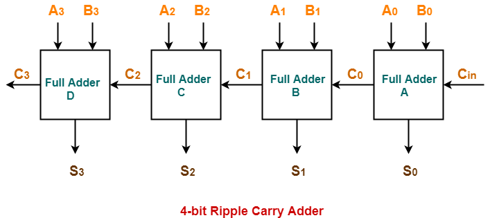
As the diagram shows:
- The first full adder (for the least significant bit, LSB) adds , , and an initial carry-in, . This is usually set to
0for simple addition. - The carry-out from this first stage becomes the carry-in for the second full adder, which adds , , and this new carry.
- This process continues, with the carry "rippling" from one stage to the next, until the final full adder calculates the most significant bit (MSB) of the sum and the final carry-out of the entire 4-bit addition.
To see this in action, the following video provides a clear walkthrough of the structure and a practical example.
Ripple Carry Adder Explained (with Solved Example) | Working and Limitation of Ripple Carry Adder
Watch the first few minutes of "Ripple Carry Adder Explained" from the ALL ABOUT ELECTRONICS channel.
Focus on the schematic of the 4-bit adder to solidify your understanding of how the full adders are connected. Then, follow the step-by-step example of adding two 4-bit numbers. Trace how the sum and carry bits are generated at each stage.
2. The "Ripple" and Its Consequences: Propagation Delay
The name "ripple-carry adder" points to its most important characteristic and its main limitation. The final sum isn't available instantly. Why? Because the third full adder can't compute its correct result until it receives the carry from the second, which in turn must wait for the carry from the first.
This chain reaction of carries creates a propagation delay. The total time it takes for the circuit to produce a stable, correct output depends on the time it takes for the carry to ripple all the way from the LSB to the MSB.
The next segment of the video you just watched explains this critical concept of propagation delay.
Ripple Carry Adder Explained (with Solved Example) | Working and Limitation of Ripple Carry Adder
Continue watching "Ripple Carry Adder Explained".
Pay close attention to the explanation of propagation delay. The example, which assumes a 15ns delay per adder, clearly illustrates how the total delay accumulates, with the final valid output available only after 60ns.
This concept is crucial in real-world chip design. The speed of an adder can directly impact the maximum clock frequency (and thus the performance) of a processor. While a ripple-carry adder is simple, its delay makes it too slow for many high-performance applications. More advanced adders, like carry-lookahead adders, are designed specifically to overcome this delay.
3. Practical Construction in Verilog
Now let's translate the block diagram into Verilog. This aligns with your goal of learning RTL design and your preference for practical application. We will use structural Verilog, where we describe a circuit by instantiating and connecting its sub-components (modules).
This process involves two steps:
- Defining the building block: a
fulladdermodule. - Defining the main module (
ripplecarryadder_4bit) and creating four instances of thefulladderinside it, connecting them just like in the diagram.
The following reading provides the complete Verilog code for this.
4-Bit Ripple Carry Adder Verilog Code
Read the "PROGRAM" section from the CircuitVerse page.
First, review the fulladder module under "Step 1". This is the gate-level implementation of the circuit we designed in the last lesson. Next, carefully study the ripplecarryadder_4bit module under "Step 2". Pay close attention to how the four fulladder instances (FA0 through FA3) are created and connected.
Let's break down the most important part of the ripplecarryadder_4bit module: the instantiations.
module ripplecarryadder_4bit(sum, cout, a, b, cin);
    output [3:0] sum;
    output       cout;
    input  [3:0] a, b;
    input        cin;

    // Internal wires to connect the carry between stages
    wire c0, c1, c2;

    // FA0: Adds the least significant bits (LSB)
    // Takes external cin, produces sum[0] and the first internal carry c0.
    fulladder FA0(sum[0], c0, a[0], b[0], cin);

    // FA1: Adds the next bits
    // Takes carry c0 from FA0, produces sum[1] and internal carry c1.
    fulladder FA1(sum[1], c1, a[1], b[1], c0);

    // FA2: Adds the third bits
    // Takes carry c1 from FA1, produces sum[2] and internal carry c2.
    fulladder FA2(sum[2], c2, a[2], b[2], c1);

    // FA3: Adds the most significant bits (MSB)
    // Takes carry c2 from FA2, produces sum[3] and the final external cout.
    fulladder FA3(sum[3], cout, a[3], b[3], c2);

endmodule
Notice how the output port for the carry of one instance (e.g., c0 from FA0) is connected to the input port for the carry of the next instance (c0 into FA1). This is the "cascading" or "rippling" implemented in code. The signals c0, c1, and c2 are declared as wire because they are simply used to connect the modules internally.
Conclusion
In this lesson, we successfully constructed a 4-bit ripple-carry adder, scaling up from the single-bit full adder. This demonstrates a fundamental principle of digital design: building complex functionality from simple, reusable blocks.
Here are the key takeaways:
- A multi-bit ripple-carry adder is built by cascading or chaining several 1-bit full adders.
- The carry-out () of each full adder becomes the carry-in () for the next, more significant stage.
- This structure leads to propagation delay, as the carry signal must "ripple" through the entire chain before the final result is stable.
- In Verilog, this is implemented using structural modeling, where you instantiate modules and connect their ports with wires.
So far, all the circuits we've built—decoders, multiplexers, and now adders—are combinational. Their outputs depend solely on their current inputs. If you change the input, the output changes (after a propagation delay). They have no memory of past inputs.
In our next lesson, we will begin exploring sequential logic, the other major class of digital circuits. These circuits introduce the concept of state and memory, allowing us to build registers, counters, and ultimately, the complex systems that make up modern processors. We'll start by understanding the role of a clock signal and the fundamental memory element: the flip-flop.