Hello! In our last lesson, we designed a 4-bit register with a load-enable signal, creating a fundamental block for storing multi-bit data. You learned that controlling the data path with multiplexers is the standard way to decide when to store a new value, as opposed to altering the clock signal itself.
Today, we'll build upon this idea of a state-holding register to create a circuit that doesn't just store a static value but transitions through a defined sequence of values. This is the core concept of a synchronous counter. Our goal is to learn how to formally describe the behavior of such a counter using a state transition table, a tool that is central to designing any sequential logic circuit.
1. What is a Synchronous Counter?
In digital systems, a counter is a sequential circuit that proceeds through a prescribed sequence of states upon the application of input pulses. A key distinction in counter design is how the clock signal is distributed.
A synchronous counter is a counter in which all the flip-flops are triggered by the same, common clock signal. This is in contrast to an asynchronous (or ripple) counter, where the output of one flip-flop acts as the clock for the next one. For modern, high-speed applications like the ones you'll encounter in your bootcamp, synchronous design is the standard because it ensures all state changes happen at the same, predictable time, avoiding the cumulative delays that plague ripple counters.
Let's watch a brief introduction to this concept.
Synchronous Counters Explained (Part-1)
This video from ALL ABOUT ELECTRONICS introduces synchronous counters and contrasts them with the ripple counters you might see in introductory texts.
Watch the segment from the beginning that explains why synchronous counters are used for high-speed applications and outlines the general design procedure. Notice the critical feature: all flip-flops receive the clock at the same time.
2. Describing the Counter's Sequence
To design a counter, we first need a clear, unambiguous way to describe its behavior. We'll use two related tools: the state diagram and the state transition table.
- State Diagram: A visual, graphical representation. Each circle represents a state (a value the counter can hold), and arrows show the transitions between states that occur on each clock edge.
- State Transition Table: A tabular version of the state diagram. It systematically lists every possible present state and the corresponding next state the counter will transition to. This table is the foundation for deriving the logic of our circuit.
Let's look at a complete analysis of a simple 2-bit synchronous up-counter to see these concepts in action.

Focus on the State Transition Table in the bottom right of the image. Let's break it down:
- Present State (Q1, Q0): This represents the current value stored in the counter's two flip-flops.
- Next State (Q1+, Q0+): This is the target value we want the counter to hold after the next rising clock edge.
- Flip-Flop Inputs (D1, D0): This is the most important part for design. It specifies what values must be presented to the D inputs of the flip-flops right now to produce the desired next state on the upcoming clock edge.
Recall from our lessons on D flip-flops that their characteristic equation is . This makes our job simple: to get a desired next state, we just need to feed that value into the D input. Therefore, for a D flip-flop-based counter, the "Next State" columns and the "Flip-Flop Inputs" columns are identical!
3. From State Table to Logic
The state transition table is more than just a description; it's a blueprint for the combinational logic that drives the counter. Our goal is to create a circuit that generates the required D inputs based on the present state Q.
Let's use the table from the image above to derive the logic for our 2-bit counter:
| Present State (Q1 Q0) | D1 (= Q1+) | D0 (= Q0+) |
|---|---|---|
| 0 0 | 0 | 1 |
| 0 1 | 1 | 0 |
| 1 0 | 1 | 1 |
| 1 1 | 0 | 0 |
Logic for D0:
Look at the D0 column. D0 is '1' when Q0 is '0', and D0 is '0' when Q0 is '1'. This is the definition of an inverter.
Logic for D1:
Look at the D1 column. D1 is '1' when the present state is 01 or 10. This is the exclusive-OR (XOR) function.
This simple process of reading the table gives us the exact logic we need to build our counter. The final circuit in the top-left of the image Analysis of a 2-bit Synchronous Counter implements exactly these two equations, feeding the D inputs of the state register.
4. The General Model of a Sequential Circuit
The structure we've just derived—a block of flip-flops for storage (the state register) and a block of combinational logic to determine the next state—is a universal model for synchronous sequential circuits.
General Model for Synchronous Circuits
This article from "All About Circuits" introduces the general model for synchronous sequential systems.
Read the section titled "Synchronous Sequential Circuits". Pay close attention to Figure 1. It perfectly illustrates the two-part structure we've been discussing: Storage Elements: The register that holds the present_state. Next State Logic: The combinational logic that takes the present_state and produces the next_state. This model is the key to understanding and designing complex sequential systems in a structured way.
5. Creating a State Transition Table
Now that you understand the structure, let's practice creating a state transition table for a different sequence: a 3-bit down-counter. This counter will sequence from 7 down to 0 (111, 110, ..., 000) and then wrap around.
The following video walks through the design of both up and down counters. It uses JK flip-flops, which are less common in modern ASIC design. You should ignore the details about JK inputs. Your focus is only on the first two steps of the process:
- Drawing the state diagram.
- Filling out the Present State and Next State columns of the table.
Synchronous Counters Explained (Part-1)
This video demonstrates how to create state diagrams and the corresponding state tables.
First, quickly re-watch how the state diagram is drawn for a 3-bit up-counter. Now, watch the creation of the state diagram for a 3-bit down-counter. Next, observe how the Present State and Next State columns are filled for the up-counter. Finally, see the same process for the down-counter table. Again, disregard any discussion of J and K inputs. The goal is to master the skill of translating a counting sequence into a formal Present State / Next State table.
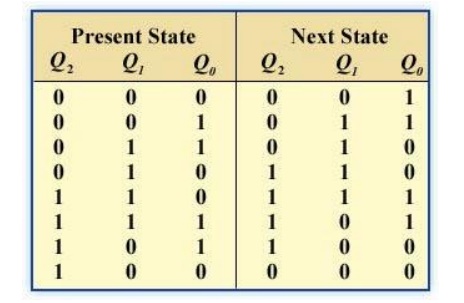
Here is another example of a state transition table for a 3-bit counter. By tracing the transitions (e.g., from 000 to 001, from 001 to 010), you can confirm this table describes a standard 3-bit up-counter.
Conclusion
In this lesson, you have learned how to describe the operation of a synchronous counter, a cornerstone of sequential logic. You've moved from the high-level idea of a counting sequence to the formal, detailed specification required to build the hardware.
Here are the key takeaways:
- Synchronous counters use a common clock for all flip-flops, making them suitable for reliable, high-speed designs.
- The behavior of a counter is visualized with a state diagram and formally defined with a state transition table.
- The state transition table lists every present state and the corresponding next state.
- For D flip-flop designs, this table directly tells us the logic required for the D inputs: the "Next State Logic" must compute the desired next state from the present state.
- This forms the fundamental design pattern for sequential circuits: a State Register (flip-flops) and Next-State Logic (combinational gates).
In our next lesson, we will begin Module 4, where you will learn the basics of the Verilog Hardware Description Language (HDL). You will see how the two-part model we studied today maps directly to a powerful and standard way of writing Verilog code to implement counters and other complex sequential machines.