Hello! In our last lesson, you learned the crucial skill of hierarchical design by instantiating one Verilog module inside another. This allows us to build complex systems from smaller, reusable blocks.
Today, we'll put that skill into practice for a fundamental part of the chip design process: verification. You'll learn how to write a testbench, a special Verilog module whose sole purpose is to test another module (your design) to ensure it behaves correctly. We will instantiate your design within this testbench and then apply a series of inputs, known as "stimulus vectors," to check its functionality.
This lesson directly addresses the learning outcome: Write a basic testbench to instantiate a design and apply stimulus vectors. By the end, you'll be able to create a framework to test any combinational logic circuit you design.
1. What is a Testbench?
Before writing any code, it's vital to understand the role of a testbench. A design module (like a multiplexer or an adder) describes hardware that can be synthesized and physically built into a chip. A testbench, on the other hand, is written only for simulation. It contains code that generates inputs and checks outputs, but it is never synthesized into hardware.
The testbench acts as a wrapper around your Design Under Test (DUT).

The core components of a simple testbench are:
- A Module Declaration: A testbench is a Verilog module, but it has no input or output ports. It is entirely self-contained.
- Signal Declarations:
- Inputs to the DUT are declared as
regtype in the testbench. This is because we will be assigning values to them within a procedural block. - Outputs from the DUT are declared as
wiretype in the testbench, as they are being driven by the DUT.
- Inputs to the DUT are declared as
- DUT Instantiation: You instantiate your design module within the testbench, just as you learned in the previous lesson. You'll use named port mapping to connect the
regandwiresignals you just declared to the DUT's ports. - Stimulus Generation: You provide a sequence of input values to the DUT to test its logic under different conditions.
2. Generating Stimulus: initial Blocks and Delays
To apply a sequence of inputs, we need two new Verilog constructs: the initial block and the delay operator (#).
How to Write a Basic Verilog Testbench
This article explains the core constructs used for generating test stimulus.
Please read the sections titled "Modelling Time in Verilog" and "Verilog initial block". Focus on: How the timescale directive defines the meaning of time units. The syntax for the delay operator (#). The fact that an initial block executes only once, starting at the beginning of the simulation.
As you read, here's a summary of the key ideas:
initialBlock: This is a procedural block that starts executing at time0of the simulation and runs through its statements sequentially, only once. This makes it perfect for defining a fixed test sequence.initial begin // Stimulus commands go here endtimescaleand Delays (#): Simulation in Verilog happens in a simulated time. The`timescaledirective, placed at the top of a file, defines the units of this time. For example,`timescale 1ns / 1psmeans that delays are measured in nanoseconds (1ns) with a precision of picoseconds (1ps).- The
#operator creates a delay.#10;pauses the execution of the block for 10 time units. We use this to hold a set of input values steady for a period before changing them to the next test vector.
- The
The image below shows a perfect example of an initial block applying a sequence of stimulus vectors to test a 3-input design. Notice how each set of inputs is followed by a #10 delay to allow time for the simulation to process the change.
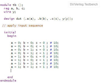
3. A Complete Testbench Example: Half Adder
Now, let's walk through creating a testbench for a simple half adder. This practical example will bring all the concepts together.
First, here is the Verilog module for our DUT, the half_adder:
// Design Under Test (DUT)
module half_adder (
    input  a,
    input  b,
    output sum,
    output carry
);
    assign {carry, sum} = a + b;
endmodule
Next, we will build a testbench to verify this half_adder. The following video provides an excellent step-by-step guide. We will focus on the testbench creation, instantiation, and stimulus generation.
verilog code for Half Adder | simulation with testbench Waveform | online simulator
This video demonstrates how to write and simulate a complete testbench for a half-adder from scratch.
Please watch the following segments: Testbench Structure: First, watch how the testbench module is defined, and how its signals are declared (reg for inputs, wire for outputs). DUT Instantiation: Next, see how the half_adder DUT is instantiated inside the testbench, connecting the testbench signals to its ports. Applying Stimulus: Pay close attention as the initial block is written to apply all four possible input combinations (00, 01, 10, 11) with delays. Observing Output (Preview): Finally, see how the $monitor system task is used to print the signal values to the console. This allows us to see the results of our stimulus. We will cover system tasks in more detail in the next lesson.
Based on the video, the complete testbench code looks like this:
`timescale 1ns / 1ps

// Testbench Module (no ports)
module half_adder_tb;

    // 1. Declare signals to connect to DUT
    // Inputs to DUT are 'reg'
    reg  a;
    reg  b;
    // Outputs from DUT are 'wire'
    wire sum;
    wire carry;

    // 2. Instantiate the Design Under Test (DUT)
    half_adder dut (
        .a      (a),
        .b      (b),
        .sum    (sum),
        .carry  (carry)
    );

    // 3. Apply stimulus
    initial begin
        // Test case 1: a=0, b=0
        a = 1'b0;
        b = 1'b0;


        #10; // Wait 10 ns

        // Test case 2: a=0, b=1
        a = 1'b0;
        b = 1'b1;


        #10; // Wait 10 ns

        // Test case 3: a=1, b=0
        a = 1'b1;
        b = 1'b0;


        #10; // Wait 10 ns

        // Test case 4: a=1, b=1
        a = 1'b1;
        b = 1'b1;


        #10; // Wait 10 ns
    end

    // 4. Observe the results (we'll study this more later)
    initial begin
        $monitor("Time=%0t ns, a=%b, b=%b, sum=%b, carry=%b",
                 $time, a, b, sum, carry);
    end

endmodule
When you run this simulation, the $monitor task would produce an output like this, allowing you to verify that for each input (a, b), the sum and carry are correct:
Time=0 ns, a=0, b=0, sum=0, carry=0
Time=10 ns, a=0, b=1, sum=1, carry=0
Time=20 ns, a=1, b=0, sum=1, carry=0
Time=30 ns, a=1, b=1, sum=0, carry=1
Conclusion
In this lesson, you've learned how to create a fundamental piece of the verification puzzle: the testbench. By writing code that exists only to test your hardware design, you can gain confidence that your logic is correct before moving on to more complex stages of the design flow.
Here are the key takeaways:
- A testbench is a non-synthesizable Verilog module used to simulate and verify a Design Under Test (DUT).
- The testbench module has no ports. It drives the DUT's inputs with
regvariables and reads its outputs withwirevariables. - The
initialblock is used to define a sequence of stimulus commands that runs once at the start of the simulation. - The delay operator (
#) is essential for controlling time and separating different input stimulus vectors.
In our next lesson, we'll expand on this foundation. You'll learn how to generate a periodic clock signal, a requirement for testing sequential circuits, and we will take a much deeper look at using system tasks like $display and $monitor to create more sophisticated testbenches.