Hello! Welcome to your next lesson in the "Embedded Interview Preparation Bootcamp."
In our last lesson, we explored watchdog timers, a critical mechanism for ensuring system-level reliability and recovery. Today, we shift our focus from internal device safety to the high-speed backbone that connects the CPU to performance-critical peripherals: the Peripheral Component Interconnect Express (PCIe). Understanding PCIe is non-negotiable for interviews at top semiconductor companies like AMD, Nvidia, and Qualcomm, as it forms the core of their SoC and GPU products.
Your learning outcome for this lesson is to: Analyze high-speed interface concepts, such as PCIe enumeration and MSI/MSI-X interrupts.
We will break this down into two key parts. First, we'll explore how a system discovers and configures devices on the PCIe bus—the enumeration process. Second, we'll dive into the modern interrupt mechanisms that make PCIe so efficient: Message Signaled Interrupts (MSI and MSI-X).
1. PCIe Fundamentals and Bus Enumeration
PCIe is a high-speed, serial, point-to-point communication standard. Unlike older parallel buses (like PCI) where devices shared a common set of wires, each PCIe link is a dedicated connection between two devices, creating a hierarchical or "tree-like" topology.
To get a quick refresher on what PCIe is and its basic structure, please start with this video.
This video from Texas Instruments provides a concise introduction to PCIe, its evolution from parallel PCI, and its core hierarchical components.
Watch from the beginning to 03:32. Focus on: The shift from parallel to high-speed serial communication. The key components: Root Complex (connects CPU to the PCIe fabric), Endpoint (the device itself, like a GPU or NVMe drive), and Switches (which expand the bus, similar to a network switch).
The Enumeration Process: How the System Builds the Device Tree
When a system boots, the host CPU has no knowledge of what devices are connected to the PCIe bus. The process of discovering, identifying, and configuring these devices is called enumeration. This process is managed by system firmware (like BIOS/UEFI) or the operating system.
Enumeration is essentially a depth-first search of the PCIe device tree, starting from the Root Complex. Each function on a PCIe device is identified by a unique address composed of three parts: Bus, Device, and Function (BDF).
- Bus Number: Identifies a specific PCIe bus segment. The Root Complex sits on Bus 0.
- Device Number: Identifies a specific device slot on a bus (0-31).
- Function Number: A single physical device can contain multiple independent functions (0-7), e.g., a multifunction card.
The host software systematically scans every possible BDF combination. When it finds a device, it reads its Configuration Space, a set of standardized registers that describe the device's identity (Vendor ID, Device ID), capabilities, and resource requirements.

To understand the step-by-step logic of enumeration and resource assignment, let's turn to a technical document.
[PDF] PCI-Express introduction
This NXP document, 'PCI-Express introduction', provides a clear, technical summary of the enumeration process and interrupt mechanisms.
Please read section 4, 'PCIe enumeration and resource assignment'. Focus on the two main phases described: Discovery (the first set of bullet points): The depth-first traversal using BDF to find devices and read their Header Type and BARs. Resource Assignment (the second set of bullet points): How the host software calculates the required memory/IO space and programs the Base Address Registers (BARs) of each device, effectively mapping it into the system's address space.
The key steps in enumeration are:
- Scan: The host probes BDF 0:0:0.
- Identify: It reads the Vendor and Device IDs. If they are not all
0xFFs, a device is present. - Classify: It reads the Header Type. If it's a standard Endpoint (Type 0), it reads its resource needs from its Base Address Registers (BARs). If it's a Switch/Bridge (Type 1), the host assigns a new
Secondary Bus Numberto the downstream link and updates theSubordinate Bus Numberto define the range of buses behind the bridge. It then recursively continues the scan on that new secondary bus. - Allocate: After the entire tree has been scanned, the host software allocates non-overlapping memory and I/O address ranges to each device by writing the physical base addresses back into their BARs.
At the end of this process, every device is discovered, identified, and mapped into the system's memory. Now, how do these devices signal events to the CPU?
2. PCIe Interrupts: MSI and MSI-X
In legacy systems, interrupts were handled by dedicated physical wires (IRQ lines). This model has severe limitations, including a finite number of lines and the complexity of sharing lines between multiple devices.
PCIe introduced a far more scalable and efficient method: Message Signaled Interrupts (MSI). Instead of asserting a physical wire, a device generates an interrupt by writing a small data packet (a message) to a specific memory address.
This video gives a great conceptual overview of why MSIs were introduced.
How Interrupts Work in Modern Computers
This video from BitLemon explains the fundamental shift from polling and physical IRQ lines to message-based interrupts.
Watch from 03:16 to 05:35. Pay close attention to the visual distinction between dedicated IRQ lines and Message Signaled Interrupts (MSI) being delivered over the PCIe bus, just like any other data.
Now, let's dive into the technical details and distinctions that are crucial for an interview.
What do the different interrupts in PCIe do?
This Stack Exchange answer provides an exceptionally detailed history and technical breakdown of INTx, MSI, and MSI-X. This level of detail is exactly what differentiates a senior candidate in an interview.
This is a dense but highly valuable read. Please focus on the main answer by user 'Frr' and the final clarifying comment. INTx (Legacy) Section: Understand that in PCIe, legacy INTx interrupts are not physical wires. They are special in-band Assert_INTx / Deassert_INTx messages that simulate the behavior of the old wires. MSI Section: Note that an MSI is a simple memory write transaction. The OS programs the device with a target address and data value. This eliminates sharing and the need for the ISR to poll devices to find the interrupt source. MSI-X Section: Grasp the key advantage: a single device function can have multiple (up to 2048) interrupt vectors. This is critical for high-performance devices with multiple queues (e.g., a network card with separate interrupts for each TX/RX queue). Final Comment: The short answer by 'sagar' perfectly summarizes the distinction: INTx are messages, while MSI/MSI-X are posted memory writes.
INTx, MSI, and MSI-X: The Comparison
Here is a summary table to consolidate your understanding. This is prime interview material.
| Feature | INTx (in PCIe) | MSI (Message Signaled Interrupts) | MSI-X (Extended MSI) |
|---|---|---|---|
| Mechanism | In-band Assert/Deassert messages. |
A single memory write Transaction Layer Packet (TLP). | Multiple, independent memory write TLPs. |
| Signaling | Virtual level-triggered logic (simulates a wire being held high/low). | Edge-triggered (the write event itself is the interrupt). | Edge-triggered. |
| Sharing | High potential for sharing a virtual wire, requiring the OS to poll devices. | Generally no sharing. One device function gets its own vector. | No sharing. Each interrupt source within a device gets its own vector. |
| # Interrupts / Func | 1 (mapped to one of 4 virtual wires A-D). | 1 (can be expanded to 32, but rarely used). | Up to 2048, highly granular. |
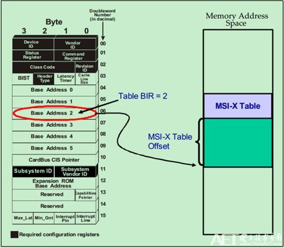
| Configuration | Complex virtual wire "swizzling" and merging in switches/bridges. | OS writes a target address/data pair into the device's config space. | OS finds the MSI-X table in memory via a BAR, then programs each entry in the table. |
| Primary Use Case | Legacy hardware/software compatibility. | General-purpose PCIe devices. | High-performance devices with multiple queues (NVMe SSDs, NICs, GPUs). |
To visualize how MSI-X works, consider this diagram:
Conclusion
Key Takeaways:
- PCIe Enumeration is a standardized, depth-first discovery process where the host software scans for devices using a Bus-Device-Function (BDF) addressing scheme, reads their capabilities from the configuration space, and maps them into system memory by programming their Base Address Registers (BARs).
- Message Signaled Interrupts (MSI) replaced legacy wired interrupts. Instead of using a physical wire, a device triggers an interrupt by performing a memory write to a specific address, which is intercepted by the CPU's interrupt controller.
- MSI-X is an extension of MSI that allows a single device function to have up to 2048 independent interrupt vectors. This is essential for modern, high-performance hardware, as it allows for fine-grained signaling from multiple internal sources (like queues) without any software polling.
- Crucially, even legacy INTx support in PCIe is handled via in-band messages, not physical wires.
Preview of the Next Lesson:
We've just completed our deep dive into the hardware protocols that form the nervous system of a modern computer. We'll now transition to the software that tames this complex hardware. In our next module, "System Design for Embedded Applications," we will start by learning how to design a portable Hardware Abstraction Layer (HAL) API using function pointer structures, a fundamental technique for writing clean, reusable embedded software.